0
\$\begingroup\$

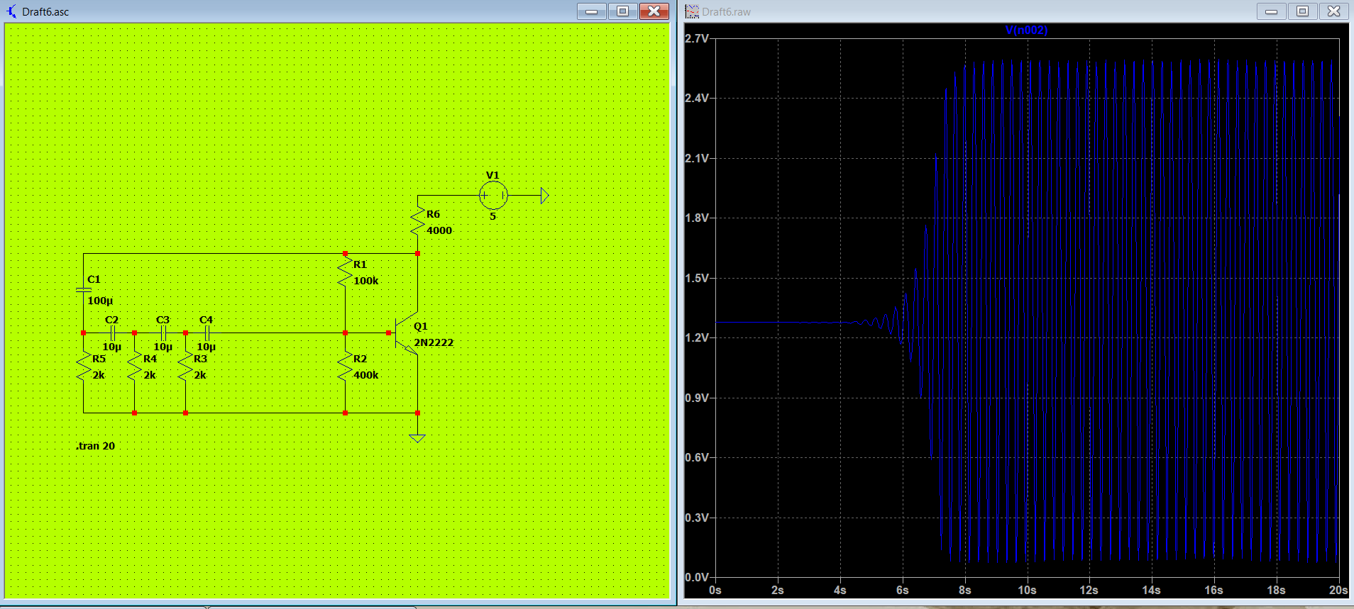
I am trying to make an oscillator circuit in real life, so I am using LTspice to simulate it, but I really don't understand the criterion for making the circuit oscillate. I understand the operating principle of the phase shift system, that is totally fine. The circuit below oscillates fine

First circuit that works

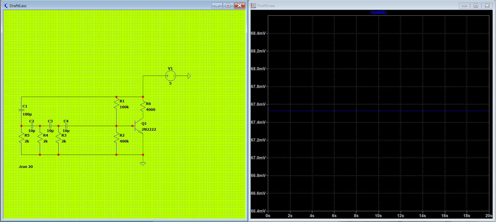
But when I change the placement of the R6 resistor and make it parallel with R1, it stops oscillating. What exactly changes with this placement ? I know gain equals \$-g_m \cdot R_c\$, but \$R_c\$ stays the same in both configuration, so gain should also stay the same, therefore it should not change anything? Obviously I am wrong, I just want to know where exactly I am wrong.

Aside from that, maybe it does affect the biasing of the circuit? Does it enter saturation when I do that? How do you go about calculating the biasing?

Second circuit that does not work

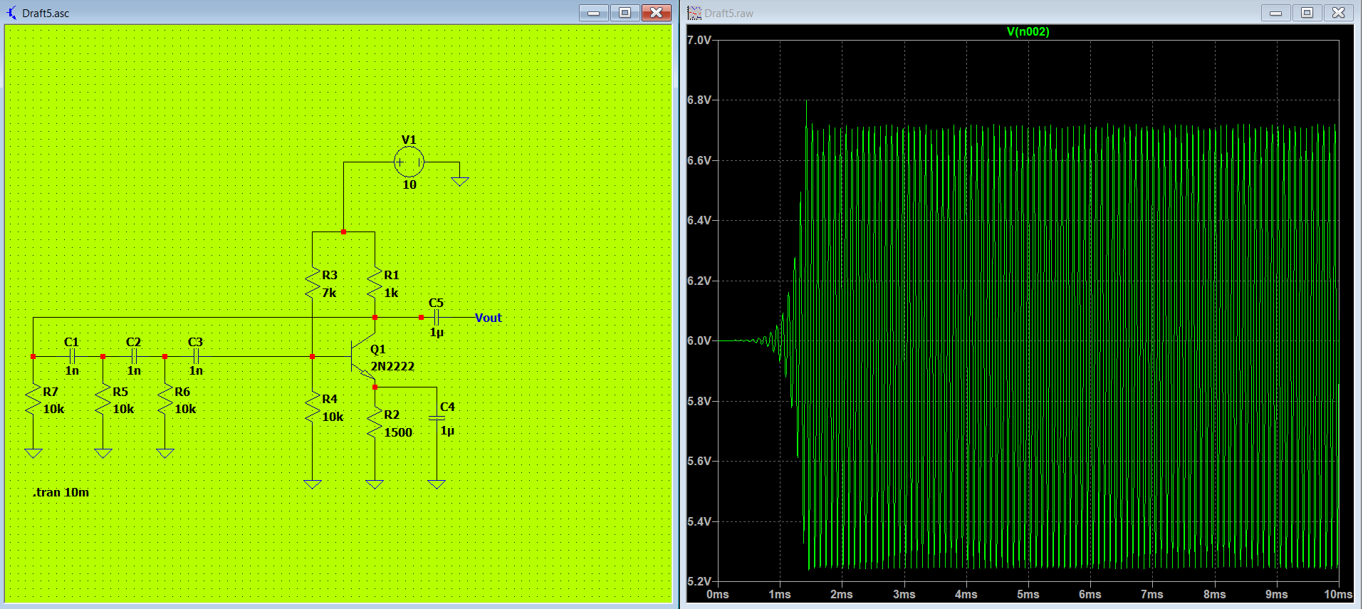
So overall, I really want to know how to dimension these resistor values. I also copied another circuit that works totally fine, but looks completely different. In this circuit, when I delete the bypass capacitor C4 or change the value of R2 too much the circuit stops oscillating, but there was not even need for these in the above circuits.

I am very confused about this topic, I will appreciate any help.

Third circuit

\$\endgroup\$
7
  • \$\begingroup\$ Please consider reading something I recently wrote. It may help a little. \$\endgroup\$ Commented Aug 21 at 4:08
  • 1
    \$\begingroup\$ @periblepsis thank you so much, from all of the answers i looked up yours was the most helpful. Because you explained the mathematical derivation, now i designed the circuit i want in the frequency i want, very helpful. But i still would like to know the reason for your choice in collector and base current, is the ratio between them are important ? or the magnitude of them also play a part ? thats what i'd like to know next. \$\endgroup\$ Commented Aug 26 at 1:40
  • \$\begingroup\$ The ratio of collector to base current is \$\beta\$ or \$h_{_\text{FE}}\$ (depending on what's under discussion.) You want a circuit that does not depend highly upon any specific value. So you do not want it to be important and you design the circuit so that its importance is low. Still, you do have to depend upon some value. The quiescent operating point is usually chosen based upon what the circuit will drive and the transistor is then selected that is a good match with this need. However, parasitics matter. So does frequency. So there's no bright line here. Thinking is always needed. \$\endgroup\$ Commented Aug 26 at 2:16
  • \$\begingroup\$ As I mentioned in that answer, if you use a solderless breadboard then this will require capacitor values that are large enough that the breadboard's parasitics don't matter. Sadly, together with typical bipolar parasitics and good operating points this also means high predictable frequencies are difficult to achieve on a solderless breadboard. Perhaps 10 kHz if you run it cooler. If you run it hot, you might push towards 100 kHz, predictably. Beyond that, it's hit and miss I think. Or much more complex to analyze, anyway. Solderless breadboards are mostly for audio frequencies. \$\endgroup\$ Commented Aug 26 at 2:27
  • 1
    \$\begingroup\$ @periblepsis thanks for the detailed explanation once more. \$\endgroup\$ Commented Aug 26 at 3:02

2 Answers 2

1
\$\begingroup\$

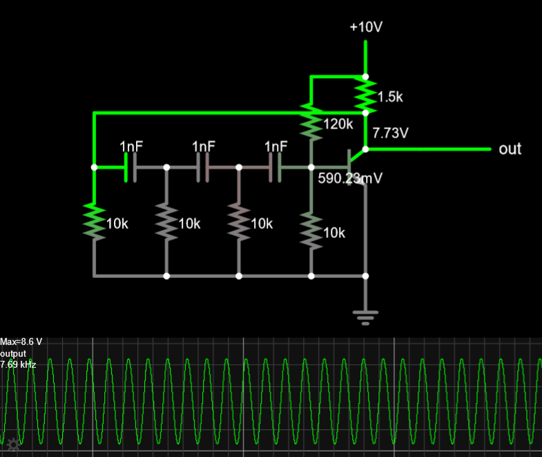
The requirement for the phase shift oscillator is to have 180 phase shift after the collector to base and have enough Av- gain to overcome the loss with a gain of almost 100 or 40 dB.

H biased gives more attenuation but is no more DC stable or centred at Vc= Vcc/2 but at least the current is regulated better.

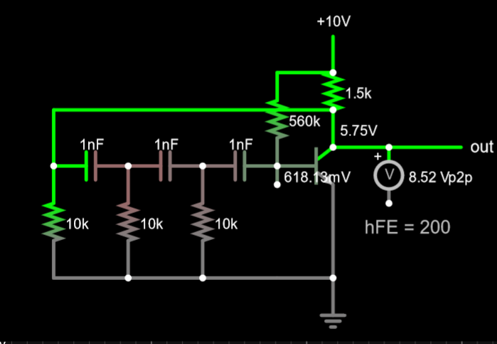
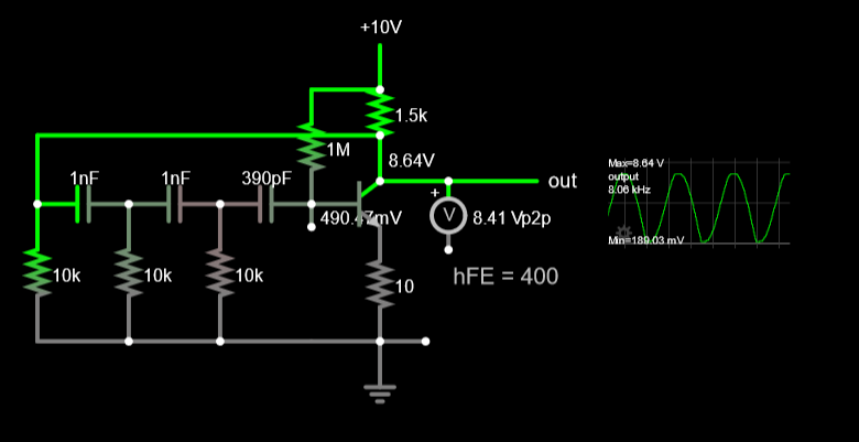
The values for Rb (up), Rc, Vcc and hFE are sensitive to optimize swing output to get any oscillation. If the output is too low, the Ib is too high. If the swing is too small then the hFE/ loss is not enough > 1. hFE is current sensitive and there tends to be an optimal mid-range current for each device to get max. hFE.

This design is much easier using an Op Amp.

This design is marginal for gain the best I could get with these filter values was 80% of Vcc which was more than LTspice.

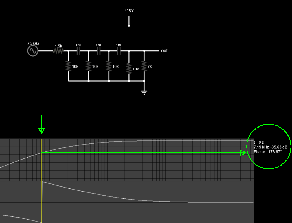
Below is the Bode plot for the filter and the time domain simulation using Falstad's tools.

You can work out the math faster than I can optimize it.

https://tinyurl.com/22b4objt

enter image description here

enter image description here

enter image description here

2N5088 NPN enter image description here

\$\endgroup\$
2
\$\begingroup\$

The second circuit doesn’t oscillate because there’s no feedback, you’ve connected C1 directly to your supply voltage.

\$\endgroup\$

Your Answer

By clicking “Post Your Answer”, you agree to our terms of service and acknowledge you have read our privacy policy.

Not the answer you're looking for? Browse other questions tagged or ask your own question.