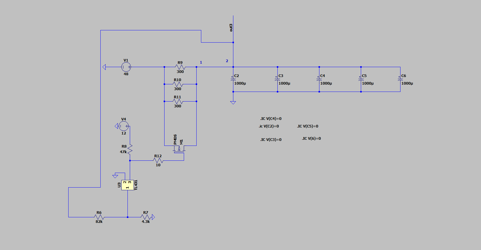
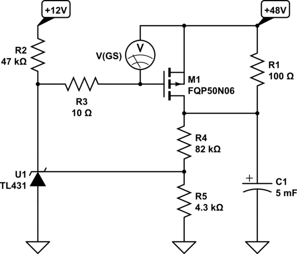
Unfortunately, the circuit has no chance of working as shown. It is very important to draw the schematic in a way that makes the function easy to see. Here's a redrawn schematic of the "Youtube" approach:

simulate this circuit – Schematic created using CircuitLab
As you can hopefully see, the TL431 is not regulating any current. Its feedback is just the capacitor voltage. So, TL431 will regulate the voltage on C1 - it will attempt to charge C1 as quickly as possible, with inrush limited only by parasitic impedances and ESRs in the circuit.
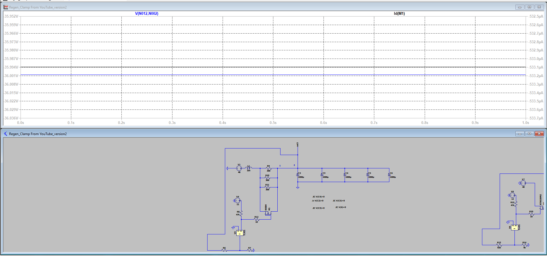
The circuit works some way I want to know is this works really like this.
You show that the circuit does not work, and that is correct. The "some way" it works is just not... :(
You claim that you have "designed" the circuit, but all you really did was copy it from someone's video, without understanding. That's not design, that's cargo cult. There are very many "Youtube circuits" that have the sole purpose of generating views. Note how generating views has nothing to do with whether the circuit is any good or if it even works. And people pointing out the circuit's shortcomings generate "engagement" that makes the video with the bad circuit even more visible. It's an unfortunate situation, ripe for abuse.
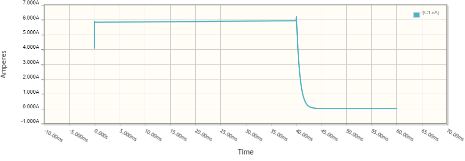
Below is a circuit that would do the job of limiting the current to 6A whether during inrush or during normal operation. It would also need thermal protection for M1. There are mosfets with a built-in temperature sensing junction that could be used for that. Otherwise, a temperature-sensing transistor would need to be thermally coupled to M1 and used to turn off the mosfet when it got too hot relative ambient air. During inrush, R4 dissipates ≈5W, but this lasts less than 0.1s:


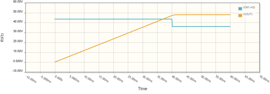
If you only need inrush protection and not continuous protection, then there is a lower cost circuit available that controls the slew rate of C1 rather than the charging current. Since that circuit doesn't act as a fuse, it won't need thermal protection for the mosfet. The mosfet will be fully on (short-circuit) after the initial charging of the capacitor. The mosfet still needs some heat sinking to dissipate the ≈0.5J of heat it generates each time the circuit is turned on with the capacitor discharged.

simulate this circuit

