0
\$\begingroup\$

I am inexperienced. I am worried the traces are too long.
And I worry about the high frequency SPI lines.
I worry that they might cause emi not work properly.

So, is this PCB layout reasonable?

I have SCK and Data lines highlighted in green.
The other lines are mostly chip select lines.
The traces are a bit thick 0.4mm because of physical durability concerns. The sensors are on the red side.
Both sides have a ground plane.
3.3v logic. 8Mhz clock. On the blue side is one esp32 s3 collecting data and sending it back out to a second stacked esp32 s3.
Cropped out is a two row button matrix and argb to match.

The whole cycle is ~600 Milliseconds

  1. trigger sensors to start collecting.
  2. send old sensor data over spi to second stacked esp32.
  3. Write 1 or 2 lines to oled Display
  4. trigger sensors to return their data

if it matters this is the sensor https://www.lcsc.com/product-detail/Position-Sensors_Infineon-Technologies-TLE5012BE1000_C123083.html

Basically what I am asking is, does this PCB look sketchy or reasonable?

PCB Layout

\$\endgroup\$
3
  • \$\begingroup\$ The length is less relevant than the fanout here. \$\endgroup\$ Commented Sep 13 at 12:32
  • 1
    \$\begingroup\$ Putting vias in the pads will either increase the cost of your PCB (for filled & plated vias) or make it harder to solder properly (when all the solder runs into the via instead of staying on the pad). Is not like you're pressed for space - move the vias off the pads. \$\endgroup\$
    – brhans
    Commented Sep 13 at 15:03
  • \$\begingroup\$ You could add 20+ GND vias all around the board. \$\endgroup\$
    – Jens
    Commented Sep 13 at 16:11

1 Answer 1

1
\$\begingroup\$

Basically what I am asking is, does this PCB look sketchy or reasonable?
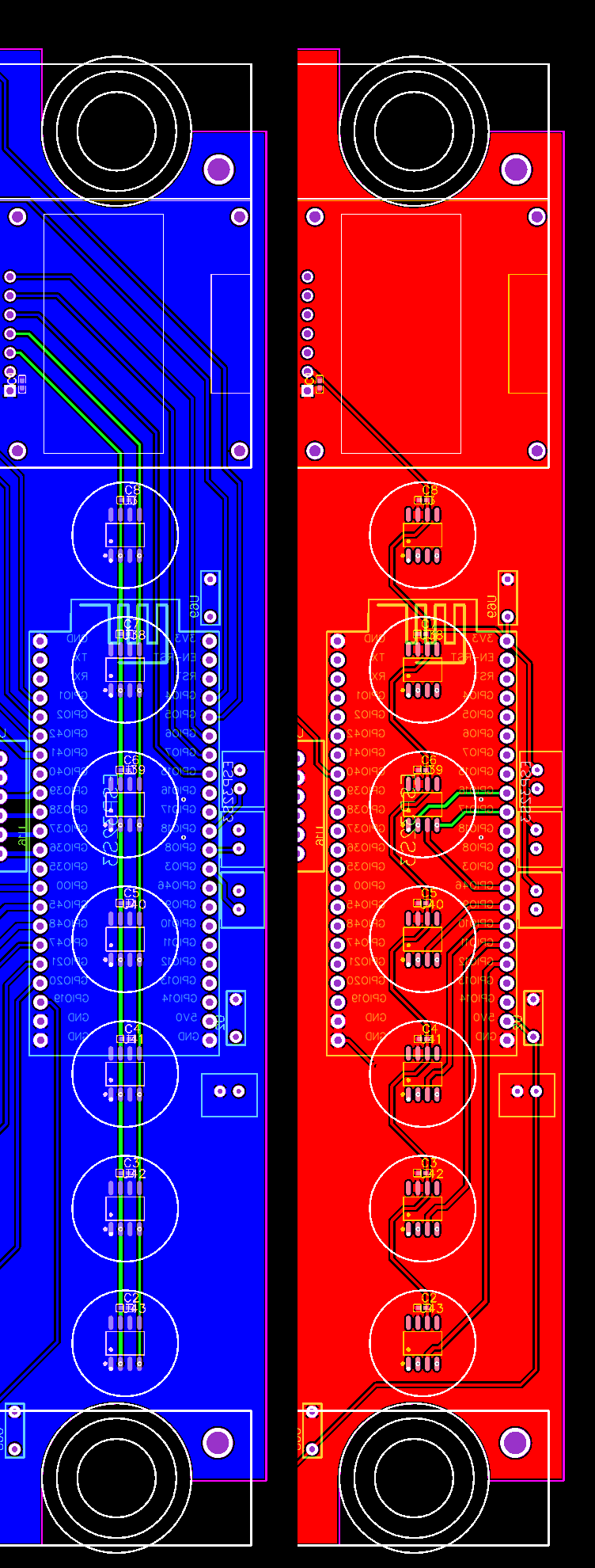
If you are worried that the tracks are too long why not squeeze all the chips up a bit. I say a bit but, there's loads of squeezing you can do from what I can see. I reckon you could reduce the overall length down to less than half without any real effort.

Keep a full ground plane on one side rather than a badly compromised ground plane on two sides.

\$\endgroup\$
1
  • \$\begingroup\$ The sensor IC need to remain where they are to detect the magnets placed above those locations. They can be rotated. I could connect them to ground with via. I will take into consideration moving more lines to one side. I just thought that more copper on the board would help with EMI when placed between traces. I made sure the design would work with ground traces and then added a copper ground plane after. \$\endgroup\$
    – Audo Voice
    Commented Sep 13 at 10:42

Your Answer

By clicking “Post Your Answer”, you agree to our terms of service and acknowledge you have read our privacy policy.

Not the answer you're looking for? Browse other questions tagged or ask your own question.