I am again looking at the operation Figure 11-1 Read Manufacturer and Device ID Signal; however, do note that in the example below, I make no effort to read the MISO data anywhere on the FPGA - I am simply trying to observe if any data is returned via the physical MISO pin from the flash device.
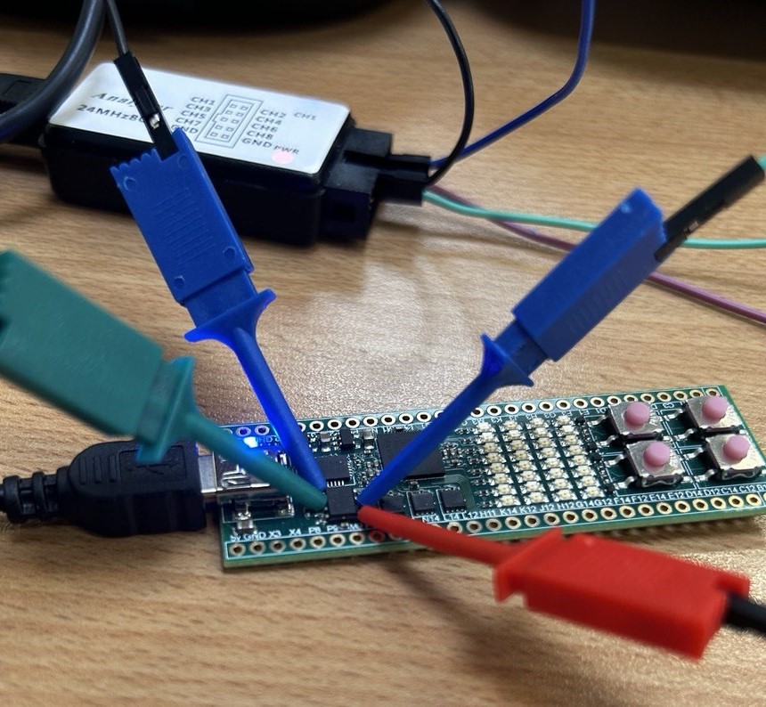
For this, I put together a logic-analyzer setup in order to observe in real time the operation - this is how the 'lab' is set-up:
The output of the logic analyzer:
The logic analyzer is connected to the SPI Flash bus as followed:
- (CH1)
D0->SCK - (CH2)
D1->CS - (CH5)
D4->MOSI - (CH6)
D5->MISO
For reference, I also posted here about the timings of the SPI operation - the above logic-analyzer output suggests that the input timings are indeed conformant to this.
However, as can be seen there are no changes at all on MISO. This mirrors the finding of my previous attempt to get a response from MISO here.
The binary on the FPGA is as followed:
module top (
    input                    clk,            // Clock input
    output                   cs,             // Chip select signal for SPI
    output                   sck,            // Serial clock for SPI
    input                    miso,           // Master In Slave Out (data from SPI device)
    output                   mosi            // Master Out Slave In (data to SPI device)
);

    // System clock counter and control for delay before starting SPI operation
    reg [7:0] clock_counter;                  // 8-bit clock counter for timing

    // SPI-related registers and flags
    reg start_flash;                          // Flag to start SPI flash read operation

    reg cs_register, mosi_register, sck_register;  // Registers for SPI control signals
    assign cs = cs_register;                  // Assign chip select signal
    assign mosi = mosi_register;              // Assign MOSI signal
    assign sck = sck_register;                // Assign SCK signal

    // SPI operation counters and opcode
    integer OPERATION_LENGTH;                 // Counter for the length of the SPI operation
    integer SI_PULSE;                         // Counter for outgoing data bits (MOSI)
    integer SO_SAMPLE;                        // Counter for incoming data bits (MISO)
    reg [7:0] OPCODE;                         // 8-bit SPI opcode for the flash memory command

    // Initial block to set default/reset states at simulation or reset
    initial begin
        // Initialize clock and LED states
        clock_counter <= 0;                   // Reset clock counter

        // Initialize SPI states
        start_flash <= 0;                     // Don't start SPI flash read yet

        // Set default states for SPI signals
        sck_register <= 1;                    // Set SCK to high (idle)
        cs_register <= 1;                     // Set chip select to high (inactive)
        mosi_register <= 1;                   // Set MOSI to high

        // Initialize SPI operation variables
        OPERATION_LENGTH <= 0;                // Initialize operation length counter
        SI_PULSE <= 0;                        // Reset outgoing data bit counter
        SO_SAMPLE <= 0;                       // Reset incoming data bit counter
        OPCODE <= 8'b10011111;                // Set SPI command (9Fh for "Read ID")
        //OPCODE <= 8'h05;                      // Set SPI command (hex 0000 0101 for "Read Status Register Byte 1")
        //OPCODE <= 8'h35;                      // Set SPI command (hex 0011 0101 for "Read Status Register Byte 2")
    end

    // Process to control the clock counter and start SPI operation
    always @ (posedge clk) begin
        if (clock_counter < 10) begin
            clock_counter <= clock_counter + 1;    // Increment clock counter
        end else if (clock_counter == 10) begin
            start_flash <= 1;                      // Start SPI flash read
        end
        if (OPERATION_LENGTH == 43) begin
            start_flash <= 0;                      // Stop SPI operation after 43 cycles
            clock_counter <= 0;                    // Reset clock counter
        end
    end

    // SPI operation logic on negative clock edge
    always @ (negedge clk) begin
        if (start_flash == 1) begin
            OPERATION_LENGTH <= OPERATION_LENGTH + 1;   // Increment SPI operation length
            if (OPERATION_LENGTH == 0) begin
                cs_register <= 0;                       // Assert chip select (low)
                SI_PULSE <= SI_PULSE + 1;               // Increment outgoing bit counter
            end
            if (OPERATION_LENGTH > 0 && OPERATION_LENGTH < 8) begin
                SI_PULSE <= SI_PULSE + 1;               // Continue sending opcode bits
                mosi_register <= OPCODE[7-SI_PULSE];    // Send opcode bit by bit (MSB first)
            end
            if (OPERATION_LENGTH >= 8 ) begin
                SI_PULSE <= 0;                          // Reset SI_PULSE counter after sending opcode
            end
            if (OPERATION_LENGTH == 32) begin
                cs_register <= 1;                       // Deassert chip select (high) after operation
            end
            // wait for some time before starting again the operation
            if (OPERATION_LENGTH == 42) begin
                OPERATION_LENGTH <= 0;                  // Reset operation length counter
            end
        end
    end

    // Clock assignment for the SPI clock (SCK) signal
    always @(*) begin
        sck_register = clk;                             // Set SCK to match the system clock
    end

endmodule
As far as I can tell - I have not made an error implementing this operation. However, the lack of a response from the chip on MISO would suggest that I have made an error somewhere.
What should I do now?
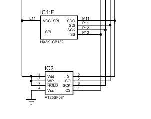
This is the config file I am using to specify connection between the FPGA pins and the Verilog code:
set_io --warn-no-port clk           P7
set_io --warn-no-port cs            P13
set_io --warn-no-port sck           P12
set_io --warn-no-port miso          P11
set_io --warn-no-port mosi          M11
From the iceFUN doc - this is how the flash is wired to the FPGA. Weirdly, it does look like the HOLD and WP pins are connected via a single FPGA output pin:


