6
\$\begingroup\$

Bus-connected devices almost always have a "high-impendance state", but I don't find where in the data sheet this is really defined. My question is this: what does an input see when connected to a Hi-Z output?

I'm considering for concrete purposes 74HCT-series parts, but I'm trying to understand how to answer the question for different logic families.

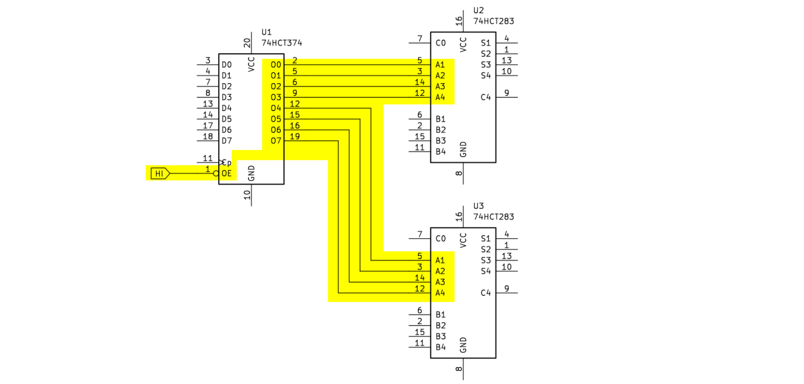
Circuit in question: where U1./OE is high, so the outputs O0-7 are "high-impedance". What does U2.A1 etc see? Logic 1? Logic 0? It looks unreliable, but I can't answer myself exactly why.

The 74HCT374 datasheet says the output leakage current is typ 5μA and the 74HCT283 datasheet says the input leakage current is typ 1μA. Does that mean it sees a logic 1?

Am I completely in the wrong place?

It's a real circuit: trying to implement a mechanism to choose value of register U1 or a constant -1 into the adder.

enter image description here

\$\endgroup\$
2
  • \$\begingroup\$ "It's a real circuit: trying to implement [...]". Is it correct to assume that this is some design you found, with the described intent, but not an idea you are trying to implement? If it is a real existing device it would be interesting to test it to see if it actually hold the lines, for some odd and undocumented reason, at 1 and for how long. \$\endgroup\$
    – devnull
    Commented Nov 1 at 15:53
  • 1
    \$\begingroup\$ @devnull sorry if I wasn't clear: by "real" I mean it's not an exercise; it was a "I wonder if this would work" idea I had. Given my ignorance of what the floating inputs will do, I thought I'd ask about it. \$\endgroup\$
    – jonathanjo
    Commented Nov 1 at 19:51

3 Answers 3

8
\$\begingroup\$

My question is this: what does an input see when connected to a Hi-Z output?

An almost perfect open circuit.

U1 is called a "tri-state" device. Each output pin has three defined conditions: logical high, logical low, and a very high impedance that cannot be relied on to either source or sink current. In the device output stage, both the pull-up and pull-down transistors are off.

Note that the 374 output leakage current is specified as "+/-". This means that for a "typical" part, the output current can be anything between +5 and -5 uA. This is a clear indication that any inputs connected to these outputs must be terminated through a less-than-infinite impedance path to a defined voltage level that complies with the input voltage specifications

If you want a downstream device to see a particular bit pattern when the 374 is in the tri-state condition, you can add high-value pull-up and pull-down resistors to the data path. For example, 10K to 100K resistors are small enough to be overpowered (safely) by the 374 output stage when active, and provide stable input termination when the 374 is in tri-state.

Gold star for providing datasheet links without prompting.

Clarity: If the B inputs all are at 0 and the A inputs are floating (due to the 374 tri-state condition), the S outputs will be a random number. Due to input stage capacitance, there will be a time period during which the A inputs will "see" the last valid states from the 374 before those outputs went tri-state, but the capacitances are so small and the input impedances are so high that someone walking past the circuit will affect the input states.

[Added from comment on other answer] Unlike a TTL input stage, a CMOS input stage has no implicit bias toward either logic state. If a CMOS input ls left floating, the potential at the input pin will be somewhere between Vdd and GND. If it drifts to something around 50% of Vdd, it is possible for both pull-up and pull-down transistors in internal stages to come partially on at the same time, creating a relatively high current path from Vdd to GND. This current can be high enough to cause device failure.

\$\endgroup\$
5
  • \$\begingroup\$ Thanks for such helpful post but it doesn't quite answer what U2, U3 will do. To be concrete, if U2.B1-4 and C0 are 0, what do we expect at U2.S1-4? \$\endgroup\$
    – jonathanjo
    Commented Nov 1 at 13:40
  • \$\begingroup\$ See the update. \$\endgroup\$
    – AnalogKid
    Commented Nov 1 at 14:19
  • 1
    \$\begingroup\$ I took the liberty of adding your excellent comment elsewhere (about current) into your answer. This is really helpful, many thanks. \$\endgroup\$
    – jonathanjo
    Commented Nov 2 at 10:11
  • 1
    \$\begingroup\$ Subsequently I found this excellent explanation from TI Implications of Slow or Floating CMOS Inputs \$\endgroup\$
    – jonathanjo
    Commented Nov 11 at 13:04
  • \$\begingroup\$ V.e.r.y. nice... \$\endgroup\$
    – AnalogKid
    Commented Nov 11 at 14:36
4
\$\begingroup\$

what does an input see when connected to a Hi-Z output?

It sees a problem, that's what. CMOS digital inputs must never be left open. That's pretty much all there's to it. If a digital signal line is ever to be left undriven (Hi-Z), there should be a so-called keeper used that will maintain the previous state of the bus. A keeper is just a buffer with a weak output:

schematic

simulate this circuit – Schematic created using CircuitLab

When U1 drives its output with either a 1 or a 0, the keeper's output impedance is too high to affect the state of the line. The keeper is "overdriven" by U1. Soon after U1's OUT changes state, the two inverters catch up and dive R1 with the same logic state.

Once U1's output is turned off (Hi-Z), the keeper takes over driving the line via its weak output resistor R1, retaining the current state of the line. The keeper has a feedback loop so it drives R1 with the same digital state it senses. That's what maintains or "keeps" the signal state after U1 has turned its output off.

In CMOS systems, buses that get shut down for potentially long periods of time need keepers. If the buses only get undriven for short time (<1ms let's say), the keepers are not needed, as long as all the loads on the bus are CMOS and thus have very high input impedance. In that case, the parasitic capacitance of the bus maintains the most recent logic state on the bus. Of course that capacitance is minuscule and discharges over time. That's why it can only work for a short time. Otherwise, a keeper is a good idea - especially when experimenting/debugging the system where a line/bus signal may be left undriven for much longer than 1ms.

The reason for two inverters is that it's how CMOS signal buffers are implemented: they are two inverters in series, or sometimes 4 or a higher even number - depending on how heavy of a load the buffer is designed to drive.

\$\endgroup\$
5
  • 1
    \$\begingroup\$ Thanks so much for your answer: are you saying we need the keeper if we want the signal to stay stable or for some other reason like not damaging U2.input? Because in this circuit surely we could just keep /OE active? \$\endgroup\$
    – jonathanjo
    Commented Nov 1 at 14:41
  • \$\begingroup\$ If /OE is driven by a fixed voltage then there's no problem. Otherwise if you can guarantee that the lines won't be undriven for longer than say 1ms, and there are only CMOS inputs on the lines and nothing else - no pull-ups/downs etc - then that's OK too. Otherwise you need a keeper. And no pull-ups/pull-downs. That's what a keeper does, and it does it with no static power consumption. Keepers are like "pulls" that know which way to pull. \$\endgroup\$ Commented Nov 1 at 15:48
  • \$\begingroup\$ Thanks for the info regarding the "keepers". What is interesting from the original description is that the idea seems to be an easy, strange, undocumented and unreliable way to generate all 1s at the inputs of the adders. \$\endgroup\$
    – devnull
    Commented Nov 1 at 15:58
  • 1
    \$\begingroup\$ "CMOS digital inputs must never be left open" ... Otherwise what happens? \$\endgroup\$
    – jonathanjo
    Commented Nov 1 at 19:54
  • 2
    \$\begingroup\$ Unlike a TTL input stage, a CMOS input stage has no implicit bias toward either logic state. If a CMOS input ls left floating, the potential at the input pin will be somewhere between Vdd and GND. If it drifts to something around 50% of Vdd, it is possible for both pull-up and pull-down transistors in internal stages to come partially on at the same time, creating a relatively high current path from Vdd to GND. This current can be high enough to cause device failure. \$\endgroup\$
    – AnalogKid
    Commented Nov 1 at 23:08
3
\$\begingroup\$

It sees something like this:

schematic

simulate this circuit – Schematic created using CircuitLab

The 3-state output leakage current has a maximum in the datasheet, but no typical or minimum. In practice it will almost always be nA not uA, especially at room temperature.

Similarly, the capacitance has a maximum and the typical will be much less.

What this means in practice is that if you tristate an output that is connected to an input with nothing else in the circuit, the steady-state input state is undefined since the leakage can be positive or negative.

Since there's a small capacitance in the input and in the output, it may retain the previous state (whatever it was, high or low) for some period of time before changing (or staying where it is, or flipping because of noise since you now have a very high impedance node).

For example, if the output leakage is 50nA and the total capacitance (input, output and stray) is 8pF then it could change 2V in a few hundred microseconds.

So you shouldn't count on the state reading high or low if the output is tristated. Instead drive it and wait long enough for it to stabilize (nanoseconds). If you really have to have inputs connected to tristated (high-Z) outputs for significant time you probably should add pull-up or pull-down resistors. Aside from other considerations, CMOS gates (including Schmitt trigger input types) can draw significantly more current if the inputs are not close to Vdd or GND.

\$\endgroup\$
5
  • \$\begingroup\$ Your R1.left is eg U1.O0 (with /OE disabled)? Is that what you mean? \$\endgroup\$
    – jonathanjo
    Commented Nov 1 at 14:44
  • \$\begingroup\$ The only time R1 (and the diodes) come into play is if you apply a voltage to the output that is more than a few hundred mV outside the supply rails and the output is tristated (or perhaps under some similar conditions with output enabled and a relatively high current flowing to outside the supply rails so that Rds(on) of the output transistors drops more than a few hundred mV). Under normal conditions where the voltage is always within supply rails you can ignore it, and the diodes. \$\endgroup\$ Commented Nov 1 at 15:48
  • \$\begingroup\$ I'm sorry, I'm still trying to understand what portion your diagram represents. Could you stick a label somewhere? \$\endgroup\$
    – jonathanjo
    Commented Nov 1 at 19:53
  • \$\begingroup\$ @jonathanjo SE is not showing me an edit link for the schematic- a problem it seems to have from time to time. Assume the left end of the resistor is the tri-stated output. If the voltage applied is always within the supply rails, you can remove the diodes and replace the resistor with a short. \$\endgroup\$ Commented Nov 1 at 21:39
  • 1
    \$\begingroup\$ Many thanks for clarifying ... I took the liberty of editing that into the schematic, hope that's okay (and I did what you meant) \$\endgroup\$
    – jonathanjo
    Commented Nov 2 at 10:07

Your Answer

By clicking “Post Your Answer”, you agree to our terms of service and acknowledge you have read our privacy policy.

Not the answer you're looking for? Browse other questions tagged or ask your own question.