I am using a chip whose part number is ADC3444 in my design.
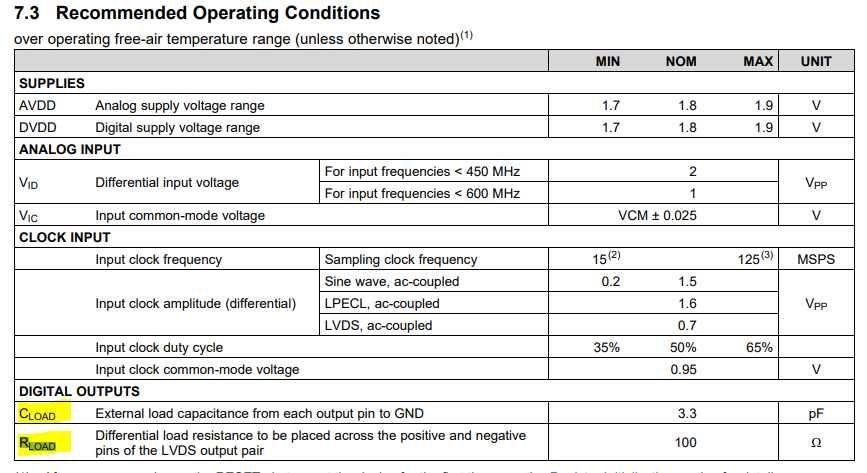
The outputs are LVDS signals. In the datasheet, it is recommended that a 100 ohm resistor needs to be placed as termination between the LVDS signal pair and an external load capacitance needs to be placed from each output pin to Ground.
The below image is from the datasheet where the above point has been mentioned.
In my application, these LVDS signals will be going to FPGA. Do i need to place the resistors and capacitors as recommended? If i don't, what might be the issues?
Kindly give a solution to my query. Thank-you
Link for datasheet:- https://www.ti.com/lit/ds/symlink/adc3444.pdf?ts=1731156418751&ref_url=https%253A%252F%252Fwww.ti.com%252Fproduct%252FADC3444

