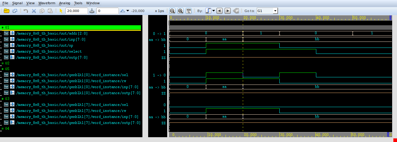
I have the task of designing an 8x8 bit memory in Verilog using CMOS. (orginally asked at Verilog - 8x8 memory unit - wrong value read, but asked to provide more details).
Currently, I have the following:
- Bitcell - takes in signals sel (if its selected), rw (read = 0, write = 1) and input. If sel=0, output is high impedance. If sel=1, it either reads, or writes (and outputs the written value).
- word_8 - Collection of 8 bitcells that also take in sel and rw (forwarded to each cell individually). 8 input and 8 output wires to each bitcell.
- decoder_3to8 - decoder that's supposed to take in an address, and select the word which is supposed to be read.
I'm running a testbench, where I try:
- Write cell 0
- Write cell 1
- Read cell 0
While the write operations work successfully, reading back from cell 0 seems to give me the value from cell 1.
My memory_8x8:
module memory_8x8 (
    input[2:0] addr,
    input[7:0] inp,
    input op,
    input select,
    output[7:0] outp
);

wire[7:0] selected_cell;

decoder_3to8 decoder(
    .valid(select),
    .addr(addr),
    .sel(selected_cell)
);

genvar i;
generate
    for (i = 0; i < 8; i = i + 1) begin
        word_8 word_instance(
            .sel(selected_cell[i]),
            .rw(op),
            .inp(inp),
            .outp(outp)
        );
    end
endgenerate

endmodule
My word_8:
module word_8 (
    input sel,
    input rw,
    input[7:0] inp,
    output[7:0] outp
);


genvar i;
generate
    for (i = 0; i < 8; i = i + 1) begin : BITCELLS
        bitcell bitcell_instance(
            .sel(sel),
            .rw(rw),
            .inp(inp[i]),
            .outp(outp[i])
        );
    end
endgenerate

endmodule
My decoder_3to8:
module decoder_3to8 (
    input valid,
    input[2:0] addr,
    output[7:0] sel
);

wire addr_NOT[2:0];


// Generate NOT addresses
not(addr_NOT[0], addr[0]);
not(addr_NOT[1], addr[1]);
not(addr_NOT[2], addr[2]);

// nb - verilog indexing reverse way - addr[0] corresponds to 00X, addr[2] is MSB
and(sel[0], addr_NOT[2], addr_NOT[1], addr_NOT[0], valid);
and(sel[1], addr_NOT[2], addr_NOT[1], addr[0], valid);
and(sel[2], addr_NOT[2], addr[1], addr_NOT[0], valid);
and(sel[3], addr_NOT[2], addr[1], addr[0], valid);
and(sel[4], addr[2], addr_NOT[1], addr_NOT[0], valid);
and(sel[5], addr[2], addr_NOT[1], addr[0], valid);
and(sel[6], addr[2], addr[1], addr_NOT[0], valid);
and(sel[7], addr[2], addr[1], addr[0], valid);

endmodule
Testbench for memory_8x8:
`timescale 1ns / 1ps

module memory_8x8_tb_basic;

  reg[2:0] addr;
  reg[7:0] inp;
  reg op;
  reg select;

  wire[7:0] outp;

  reg[7:0] expected_outp;
  integer i;

  memory_8x8 uut (
               .addr(addr),
               .inp(inp),
               .op(op),
               .select(select),
               .outp(outp)
             );

    initial begin
        $monitor("\tSelected cell: %b", uut.selected_cell);
    end

    initial begin
    // Initialize inputs
    select = 0;
    op = 0;
    addr = 3'b000;
    inp = 8'b00000000;

    expected_outp = 8'bXXXXXXXX;

    #10;

    // Stage 0
    $display("Test stage 0 - Write to cell 0, write to cell 1, read cell 0\n");

    // Write to cell 0
    select = 1;
    op = 1;
    addr = 3'b000;
    inp = 8'hAA;
    expected_outp = inp;
    #10;
    if (outp !== expected_outp) begin
        $display("Write to cell 0 FAILED at time %0t ns: Address %b, Expected %b, Got %b",
                $time, addr, expected_outp, outp);
    end else begin
        $display("Write to cell 0 PASSED at time %0t ns: Address %b, Data %b",
                $time, addr, outp);
    end

    // Write to cell 1
    addr = 3'b001;
    inp = 8'hBB;
    expected_outp = inp;
    #10;
    if (outp !== expected_outp) begin
        $display("Write to cell 1 FAILED at time %0t ns: Address %b, Expected %b, Got %b",
                $time, addr, expected_outp, outp);
    end else begin
        $display("Write to cell 1 PASSED at time %0t ns: Address %b, Data %b",
                $time, addr, outp);
    end

    // Read cell 0
    op = 0;
    addr = 3'b000;
    expected_outp = 8'hAA;
    #10;
    if (outp !== expected_outp) begin
        $display("Read cell 0 FAILED at time %0t ns: Address %b, Expected %b, Got %b",
                $time, addr, expected_outp, outp);
    end else begin
        $display("Read cell 0 PASSED at time %0t ns: Address %b, Data %b",
                $time, addr, outp);
    end

    select = 0;
    #10;

    // Read cell 2
    op = 0;
    addr = 3'b001;
    expected_outp = 8'hBB;
    #10;
    if (outp !== expected_outp) begin
        $display("Read cell 1 FAILED at time %0t ns: Address %b, Expected %b, Got %b",
                $time, addr, expected_outp, outp);
    end else begin
        $display("Read cell 1 PASSED at time %0t ns: Address %b, Data %b",
                $time, addr, outp);
    end

  $finish;

  end


endmodule
This gives the following (unexpected) output:
    Selected cell: 00000000
Test stage 0 - Write to cell 0, write to cell 1, read cell 0

        Selected cell: 00000001
Write to cell 0 PASSED at time 20000 ns: Address 000, Data 10101010
        Selected cell: 00000010
Write to cell 1 PASSED at time 30000 ns: Address 001, Data 10111011
        Selected cell: 00000001
Read cell 0 FAILED at time 40000 ns: Address 000, Expected 10101010, Got 10111011
        Selected cell: 00000000
Read cell 1 FAILED at time 60000 ns: Address 001, Expected 10111011, Got zzzzzzzz
memory_8x8_tb_basic.v:98: $finish called at 60000 (1ps)

