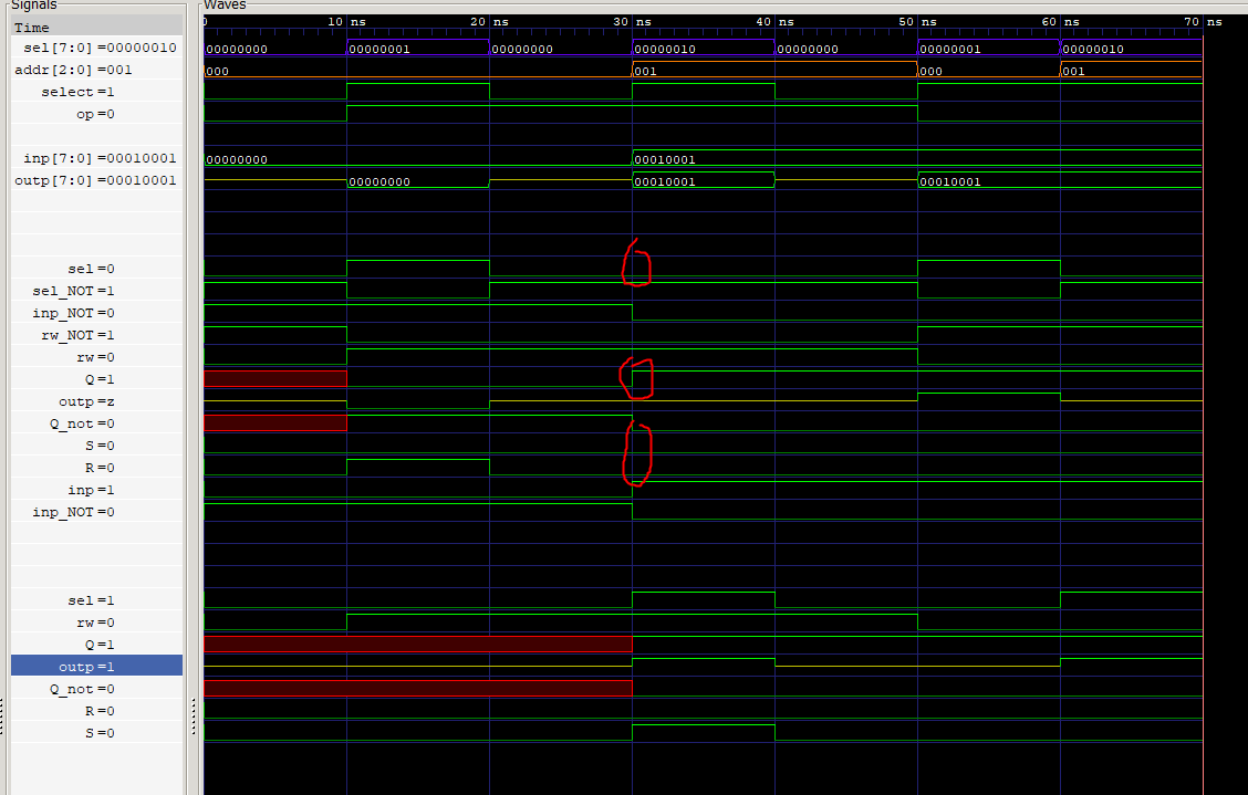
I have created an 8x8 memory module. Currently, I have the following:
- Bitcell - takes in signals sel (if its selected), rw (read = 0, write = 1) and input. If sel=0, output is high impedance. If sel=1, it either reads, or writes (and outputs the written value).
- word_8 - Collection of 8 bitcells that also take in sel and rw (forwarded to each cell individually). 8 input and 8 output wires to each bitcell.
- decoder_3to8 - decoder that's supposed to take in an address, and select the word which is supposed to be read.
- memory_8x8: 8 word_8, where the sel signals for every of them is designed using the decoder.
I run a simple test bench, where I:
- write 0x00 (0000 0000) into cell 0.
- wrote 0x10 (0001 0001) into cell 1.
- read from cell 0
- read from cell 1
Code for the testbench is:
`timescale 1ns / 1ps

module memory_8x8_tb;

  reg [2:0] addr;
  reg [7:0] inp;
  reg op;
  reg select;

  wire [7:0] outp;
  reg [7:0] expected_outp;

  // Instantiate the memory_8x8 module
  memory_8x8 uut (
    .addr(addr),
    .inp(inp),
    .op(op),
    .select(select),
    .outp(outp)
  );

  initial begin
    $dumpfile("test_stage0.vcd");
    $dumpvars();

    // Initialize inputs
    select = 0;
    op = 0;
    addr = 3'b000;
    inp = 8'b00000000;
    expected_outp = 8'bXXXXXXXX;

    #10;

    // Write 0x00 to cell 0
    select = 1;
    op = 1;  // Write operation
    addr = 3'b000;
    inp = 8'h00;
    expected_outp = inp;
    #10;

    // Verify the write to cell 0
    if (outp !== expected_outp) begin
      $display("Write to cell 0 FAILED: Expected %h, Got %h", expected_outp, outp);
    end else begin
      $display("Write to cell 0 PASSED: Data %h", outp);
    end

    // Deselect and wait
    select = 0;
    #10;

    // Write 0x11 to cell 1
    select = 1;
    addr = 3'b001;
    inp = 8'h11;
    expected_outp = inp;
    #10;

    // Verify the write to cell 1
    if (outp !== expected_outp) begin
      $display("Write to cell 1 FAILED: Expected %h, Got %h", expected_outp, outp);
    end else begin
      $display("Write to cell 1 PASSED: Data %h", outp);
    end

    // Deselect and wait
    select = 0;
    #10;

    // Read cell 0
    select = 1;
    op = 0;  // Read operation
    addr = 3'b000;
    expected_outp = 8'h00;
    #10;

    // Verify the read from cell 0
    if (outp !== expected_outp) begin
      $display("Read cell 0 FAILED: Expected %h, Got %h", expected_outp, outp);
    end else begin
      $display("Read cell 0 PASSED: Data %h", outp);
    end

    // Read cell 1
    select = 1;
    addr = 3'b001;
    expected_outp = 8'h11;
    #10;

    // Verify the read from cell 1
    if (outp !== expected_outp) begin
      $display("Read cell 1 FAILED: Expected %h, Got %h", expected_outp, outp);
    end else begin
      $display("Read cell 1 PASSED: Data %h", outp);
    end

    // End simulation
    $finish;
  end

endmodule
Now to the problem: when cell 1 is written in in step 2, the value also seems to fill cell 0, even though it is deselected.
I have dumped the test into GTKWave, and get the following:
This is a wave pattern analysis of the circuit. The upper values are for the whole memory circuit where:
- sel - selected bitcell (each bit corresponds to cell 0-7)
- addr - address (which selects the sel singal)
- sel - is any of the bitcells selected?
- op - read(0) or write(1)
The middle values are values inside of word[0], bitcell[0], and the lower ones are word1, bitcell[0].
The read areas showcase my problem. That is the moment where the selection is changed from cell 0 to cell 1, and 1 is written into the bitcell in cell 1. As one can see, sel=0 for cell 0 there. Both S and R values stay at 0, as expected. I'm using a NOR SR-latch, so this should mean the values shouldn't change. However, if you see at the Q signal, a 1 is for some reason getting written there. The output value outp still seems to be in a high impedance state as expected, but Q is getting overwritten.
The code for the bitcell is the following:
module bitcell (
    input sel, // Bitcell selected
    input rw, // 1 - write, 0 - read
    input inp,
    output outp
);

wire S, R;

wire inp_NOT;
wire rw_NOT;
wire sel_NOT;

not(inp_NOT, inp);
not(rw_NOT, rw);
not(sel_NOT, sel);

// S and R signals for NAND latch
nor s_generator(S, sel_NOT, rw_NOT, inp_NOT);
nor r_generator(R, sel_NOT, rw_NOT, inp);

// Latch
wire Q, Q_not;

nor latch_upper(Q, Q_not, R);
nor latch_lower(Q_not, Q, S);

// wire EN;
// and(EN, sel, rw_NOT);

bufif1 enable_buffer(outp, Q, sel);

endmodule
My memory_8x8:
/*
    Represents the finished 8x8 memory cell.

    Consists of 8 words of 8 bytes (word_8), selectable through 3 bit address
*/

module memory_8x8 (
    input[2:0] addr,
    input[7:0] inp,
    input op,
    input select,
    output[7:0] outp
);

wire[7:0] selected_cell;

decoder_3to8 decoder(
    .valid(select),
    .addr(addr),
    .sel(selected_cell)
);

genvar i;
generate
    for (i = 0; i < 8; i = i + 1) begin
        word_8 word_instance(
            .sel(selected_cell[i]),
            .rw(op),
            .inp(inp),
            .outp(outp)
        );
    end
endgenerate

endmodule
And word_8:
module word_8 (
    input sel,
    input rw,
    input[7:0] inp,
    output[7:0] outp
);


genvar i;
generate
    for (i = 0; i < 8; i = i + 1) begin : BITCELLS
        bitcell bitcell_instance(
            .sel(sel),
            .rw(rw),
            .inp(inp[i]),
            .outp(outp[i])
        );
    end
endgenerate

endmodule
I have now been trying for several hours to fix this, but I have no idea what might be wrong. Any ideas?

