4
\$\begingroup\$

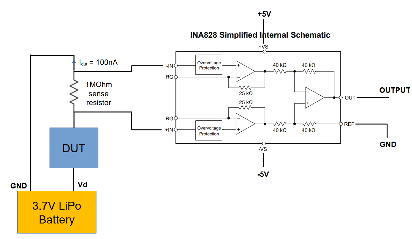
I need to measure the current draw of DUT that can be an MCU in deep sleep, such as Attiny85, or a more power hungry MCU that is powered off by TPL5110. In this post, I proposed a circuit where an INA828 is used to measure the voltage across a sensing resistor. In that circuit I proposed to have two separates grounds, one for the DUT and sensing resistor and one for the INA828. I have received very helpful comments that made me realize that the circuit would hardly work since the INA828 would very likely reach saturation due to the separate grounds.

Therefore, I propose here a new version with the hope that this will work or at least that it is an improvement compared to the previous proposal. All feedback and criticism is of course very welcome. In this version there is only a single ground. The battery is still a 3.7V LiPo. The goal is still to measure the voltage drop across a sensing resistor in order to calculate the current flowing through it. I have already realized a PCB with multiple sense resistors (from 1 MOhm down to 10 Ohm) with 0.1% tolerance and a bypass. The sense resistors can be enabled/disabled with Jumpers. I initially select the bypass to start the DUT, I put it in deep sleep and then select the appropriate sense resistor. So far I have used this test PCB and measured the voltage drop across the sense resistor using a digital multimeter (DMM). This works quite well when the current is in the order of uA or higher, but when I need to measure currents in the order of tens of nA there is a large measurement error caused by the not high enough DC input resistance of the DMM. Hence, I am looking for a buffer or OPA with larger input DC resistance than a DMM.

In this new version, see schematic below, the REF pin of the INA828 is connected to the common ground GND. The sense resistor is connected between DUT and GND. In this way, the difference between common-mode voltage and output voltage will be much smaller compared to the version I proposed in the earlier post and it should hopefully avoid saturation in the INA828, since the voltage across the sense resistor will be not more than few hundreds of mV. The +5V, -5V dual supply will be generated by two 9V batteries (to get +9V, -9V) in combination with a positive LDO and a negative LDO to convert to a "stable" +5V, -5V to avoid supply voltage drift due to 9V batteries discharging. The multiple sensing resistors with jumpers to enable/disable them would be placed in a new PCB that also includes the INA828 IC and its LDOs for dual supply.

My plan is that if I can make the INA828 circuit to work, I may connect at its output a simple DMM or an ADC. I do not need to log the data to a PC or other device, so either using DMM at the INA828 output or an ADC (for instance the ADS1263) that is controlled by an MCU with LCD display is enough for me.

  1. Do you think the schematic is correct or am I making any mistake?
  2. Is the INA828 a good choice for measuring these voltages or you have a better suggestion? My guess is that it should work well since the input bias current is 0.15nA thus negligible compared to the current flowing in the test resistor.
  3. Will I need to have galvanic isolation between the sense resistor and the OPA measuring it´s voltage? In this case I should replace the INA828 with something else.
  4. Do you agree with using a dual supply +/- 5V and to connect the REF pin to GND?

enter image description here

Thanks in advance

\$\endgroup\$
2
  • \$\begingroup\$ Bias input current can be 2 nA ... \$\endgroup\$
    – Antonio51
    Commented Nov 17 at 16:00
  • \$\begingroup\$ Do you mean that with the INA828 it will be up to 2nA? If yes, it will still not be very much considering that the minimum current I am going to measure will likely not go below 50nA. But according to the datasheet it should be 150pA. Do you have a better OPA to suggest? \$\endgroup\$
    – spanito
    Commented Nov 17 at 16:05

3 Answers 3

4
\$\begingroup\$

there is a large measurement error caused by the not high enough DC input resistance of the DMM

You're saying that the 10MΩ input resistance of a bench DMM is not high enough? That's 10V/μA sensitivity, or 10mV/nA (!). I've checked and my DMM will happily measure currents down to a fraction of a pA that way. In Volts mode.

No need for op-amps. Yes need for cleanliness. Touching the PCB may well leave enough conductive residue to obscure the results. Would be best if you had an ultrasonic cleaner and cleaned the board in isopropyl followed by deionized water. Soldering flux residue may not be great either, depending on the flux type.

The sensing resistor is the input resistance of the DMM. You can parallel something with it to yield 1MΩ parallel combination. Obviously it will be higher than 1MΩ :)

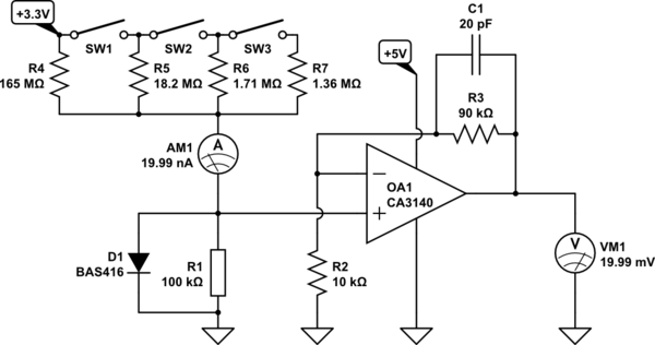
If you want to use an op-amp, a CA3130 (70s vintage) or CA3130A (slightly newer lower offset variant) will have no problem measuring things. 1MΩ input impedance is excessive though when you use an op-amp. 100kOhm, gain 10, gives 1mV/nA on the output:

schematic

simulate this circuit – Schematic created using CircuitLab

This circuit will measure up to about 4μA with reasonable accuracy. Above 4μA the diode starts shunting the sense resistor R1, keeping the CPU functional even if it happens to wake up from sleep. You may find that helpful. I certainly did :)

CA3130[A]/40[A] have offset nulling inputs. See the datasheet for how to use them. This will let you get better than 1nA accuracy at room temperature without much fuss.

CA3130[A]/40[A] also has common mode range that extends about 0.5V below ground, so this circuit will work well down to 0.0nA.

The output of the op-amp is a CMOS inverter and will swing within mV of the rails as long as it's lightly loaded.

This is a retro circuit on purpose. You can use much newer and better op-amps, but the only real improvement will come from lower input noise. I have inherited components from an old lab and have rails of those chips, thus I tend to use them. Hard to beat free :)

Also, since the circuit is so simple, you can assemble it without a PCB, just on a piece of ground plane of your choice, with teflon standoffs.

\$\endgroup\$
4
  • \$\begingroup\$ Thanks for your suggestions, especially about the cleanliness of the PCB. The reason why I would like to have the OPA between DMM and sense resistor is that I have a rather cheap and old DMM, I am a bit skeptical that its input resistance is really 10MOhm. I wanted to avoid to spend 200-300 USD/Euro in a new fancy multimeter, since I can get the PCB manufactured for very low price and the cost of the components is very low. Another reason is that the OPA will allow me to feed the output to an ADC if I need/want later on. \$\endgroup\$
    – spanito
    Commented Nov 17 at 20:00
  • 1
    \$\begingroup\$ Well, here you go, a circuit you could have built in 1970s :) \$\endgroup\$ Commented Nov 17 at 20:18
  • \$\begingroup\$ Wow, thanks a lot for the very detailed example! Sorry for my dumb question, but how do you choose the value of the capacitor C1? Is it needed for stability purposes? I think I will go for PCB anyway since it will be rather cheap. Do you have any recommendations for the PCB type? For example the substrate thickness. Typically I use 1.6mm thickness, but in this case isolation is very important so maybe a larger thickness may work better? Or am I thinking wrong? \$\endgroup\$
    – spanito
    Commented Nov 18 at 0:55
  • 1
    \$\begingroup\$ Yes, C1 is for stability. With a CA3140 it may not even be needed. Best to leave some room for it on the layout. It won't hurt and it can be used to add low-pass filtering as well. In general, the thicker the PCB, the worse it is, since it has bulk conductance - tiny but it matters once you get down to pA levels and lower. General rule with ultra low current measurements is: everything conducts. The less of it the better, usually. At nA levels it won't matter all that much unless it's crappy material like paper-phenolic. So, with FR4, regular thickness is fine. CA3130 is faster an needs C1 \$\endgroup\$ Commented Nov 18 at 14:19
3
\$\begingroup\$

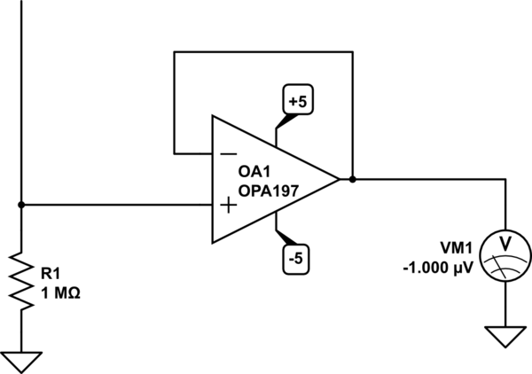
There's no need for an instrumentation amplifier in this configuration.

Just use an ordinary op-amp with +/-5V supplies, which opens up the selection considerably and removes some concerns.

schematic

simulate this circuit – Schematic created using CircuitLab

The OPA197 is one of many op-amps that will work in this application.

It is okay with the 10V supply, has a reasonably low Vos (100uV maximum at room temperature) and Vos drift with temperature and a reasonably low Ib (20pA maximum at room temperature) and isn't expensive (less than $2 one-off).

You could add some voltage gain if you wanted with a couple resistors.

The OPA197 is RRIO so you could even power it with the 3.6V battery (3.6V/GND), however it might not read correctly below 25mV = 25nA (typically 5nA) with the meter load.

P.S. I suggest an addition non-critical few kΩ resistor (say 10kΩ) in series with the non-inverting input on the above schematic, to avoid possible issues with supply sequencing). Circuitlab is not letting me edit.. and bypass capacitors, of course.

\$\endgroup\$
6
  • \$\begingroup\$ Thanks a lot for your help also in this post. As bypass capacitors is it sufficient to have both 100nF and 1uF at both V+ and V-? Considering the +5V,-5V supply I guess that 25V capacitors should be ok, do you agree or even 10V cap will be enough? I was thinking to use the negative LDO "ADP7182AUJZ-5.0-R7" and the positive LDO "ADP7142AUJZ-5.0-R7", both from AD. What do you think about them? I have selected them so far for their high PSRR and low noise. \$\endgroup\$
    – spanito
    Commented Nov 17 at 18:02
  • 2
    \$\begingroup\$ My advice is to read the regulator datasheets carefully to see what output capacitors they require. This is important. An additional 100nF/25V near the op-amp on each supply is more than adequate. \$\endgroup\$ Commented Nov 17 at 18:09
  • \$\begingroup\$ I am thinking about what will happen if the two LDOs will not give exact +5V and -5V. For instance +5.03 and -4.95. This will create an offset in the output I think. In this case there will be an imbalance and with respect to GND. What do you think would be the best approach to be able to tune the offset? Implementing adjustable LDOs with a potentiometer or using a voltage divider with trimming potentiometer? Or do you have any better suggestion for allowing tuning the offset to 0V when no current flows through the sense resistor? \$\endgroup\$
    – spanito
    Commented Nov 22 at 8:47
  • 1
    \$\begingroup\$ Oh, no. It will not create a significant offset. The op-amp has enormous rejection of power supply variations. The precision one I suggested is typically 2uV/V. So a 0.04V voltage change in a power supply will represent 80nV. \$\endgroup\$ Commented Nov 22 at 9:41
  • 1
    \$\begingroup\$ The room temperature bias current is much (30 or 70x) higher with that part, which will cause an error of 1.4mV (max) or 160uV (typical), so the offset is worse to much worse. It’s also a zero-drift part which has weirdness associated with the inputs so I would avoid for most high Z applications. \$\endgroup\$ Commented Dec 1 at 15:44
1
\$\begingroup\$

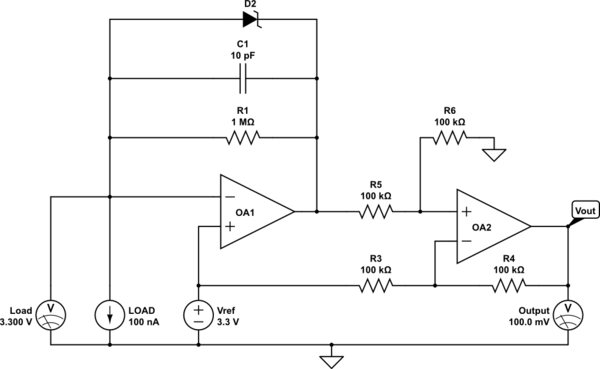
The other answers work if you don't mind the high voltage drop in the 1 Mohm resistor. But if your device sometimes draws higher current before going to sleep mode, you can use a transimpedance amplifier to provide constant supply voltage to the load.

schematic

simulate this circuit – Schematic created using CircuitLab

The opamps should be supplied with a voltage higher than the desired output voltage, for example +15V. OA1 should be selected to have high enough max output current to meet the demands of the load.

OA1 is connected as a transimpedance amplifier, and its output will be VOA1 = VREF + R1 × ILOAD. C1 acts as a low pass filter to improve stability and reduce noise.

Zener D2 is optional, but it allows the load voltage to stay in regulation even if the measurement range is exceeded. Pay attention to its leakage current, which would affect accuracy.

OA2 subtracts VREF from VOA1 and provides 1 mV per nA output.

\$\endgroup\$
4
  • 2
    \$\begingroup\$ Don't use a low voltage zener for D2 (anything <5 V), they have very high leakage at surprisignly low voltages and may cause error shunting R1. Use instead a diode-connected transistor, or even an LED, far better than a low voltage zener. OR, left-field idea here, omit R1 and use a silicon diode for D2 if you want a log-scale reading, albeit with low accuracy, though it's easy to compensate for the D2 tempco with a similar one in the other opamp leg. \$\endgroup\$
    – Neil_UK
    Commented Nov 18 at 14:01
  • 1
    \$\begingroup\$ What kind of supply voltage do you think you need for OA1, in order to keep the inverting input at 3.3V when the device is drawing "high current" in between sleep cycles? \$\endgroup\$
    – Ben Voigt
    Commented Nov 18 at 19:52
  • 1
    \$\begingroup\$ @BenVoigt Enough for opamp output to go to Vref + R1 * Iload (or Vref + V_D2 if the diode is used). Depends on opamp how much supply margin it needs to give the required output voltage at the load current. \$\endgroup\$
    – jpa
    Commented Nov 19 at 7:14
  • \$\begingroup\$ Thanks for your suggestion! \$\endgroup\$
    – spanito
    Commented Nov 19 at 18:48

Your Answer

By clicking “Post Your Answer”, you agree to our terms of service and acknowledge you have read our privacy policy.

Not the answer you're looking for? Browse other questions tagged or ask your own question.