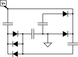
This is intended to be a voltage multiplier.
Can anyone check if my connections are correct or accurate to my schematic?
This is intended to be a voltage multiplier.
Can anyone check if my connections are correct or accurate to my schematic?
The "black input line" (Labeled "-" on your breadboard) should connect directly to four components, but I only count three.
Trick is this: while a solderless breadboard cannot be connected in arbitrary ways, you can always rearrange your schematic such that it reflects the connections on the breadboard. So, use the schematic capture software used to produce your schematic, and rearrange that, without removing connections or adding new ones between components that were formerly connected, until you get something you can plug into a circuit board, directly.
In more technical terms, while a schematic and your fritzing breadboard drawing are both representations of a circuit, the circuit functionality is defined by its connectivity graph, i.e., a list of which pins are connected to each other, and which components have which pin. You can rotate your schematic, you can stretch or shorten lines and do many things to your schematic, whithout affecting that graph. Only if your schematic and the breadboard have the same graph can the breadboard show the same circuit as your schematic.
So. First step, label the components in your breadboard image. That solves 90% of confusion. Then, for every pin in your schematic, find it in your breadboard, and make sure it's connected to exactly the same pins as in your schematic. Mark all the connections you've checked in green in your schematic, directly after checking. Mark all the components you've checked in green. When your whole schematic is green, you've verified that you've built an equivalent breadboard.
This is the circuit you have created on breadboard:

simulate this circuit – Schematic created using CircuitLab
Which probably could be drawn better but it gives me a 404 error when I try to edit it (posted too quickly) and it's not worth doing again as the breadboard has no designators so I have no idea what is supposed to be what.
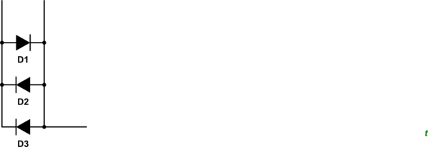
However, you can see clearly that your breadboard circuit is not what is in your schematic
Figure 1. First error.

simulate this circuit – Schematic created using CircuitLab
Figure 2. What you have made.
There are no component designators on your breadboard layout so I don't know which component is which but it is clear that you have connected three diodes in a parallel / anti-parallel arrangement which doesn't exist in your schematic.
I suggest you rip-up and retry, a common term coined in the early days of PCB layout tools.