0
\$\begingroup\$

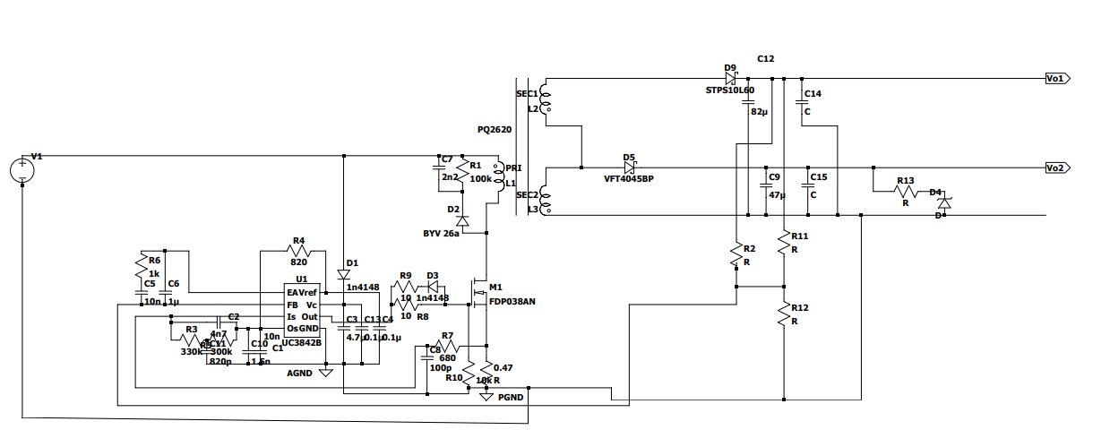
made from LTspice

I am doing an EMI filter for a step down flyback DC - DC converter 20 V to (20 V and 10 V) multiple outputs. The controller used here is UC3842. I have the following questions for making this EMI filter

  1. Any suggestions on which type of filter must be used: (Pi filter or type-2, 3 etc.)
  2. How do I select the values of the inductor and capacitor?

It would be helpful if one directs me to a reference or gives me a brief overview on how to proceed with making the EMI filter.

\$\endgroup\$
5
  • \$\begingroup\$ What problem are you trying to solve with the filter? \$\endgroup\$
    – Andy aka
    Commented Nov 21 at 10:43
  • \$\begingroup\$ we want to reduce the conducted emission of this circuit by using an emi filter. \$\endgroup\$
    – Fredrick
    Commented Nov 21 at 12:15
  • \$\begingroup\$ Filter design is a numbers and a specification game. Very little of it is down to generalities. \$\endgroup\$
    – Andy aka
    Commented Nov 21 at 12:57
  • \$\begingroup\$ I learnt that there is a mathematical transfer function we can derive from the corner frequencies of the poles and the zeros we want to plot which can attenuate the noise in the specific frequency range. but getting specific to where I want to place the poles and zeros is the hard part. maybe that can be done after the actual emi test of the pcb. it would be helpful to receive an answer which gives a reference about the poles and zeros placement and practical considerations in choosing the value of the capacitors and inductors. \$\endgroup\$
    – Fredrick
    Commented Nov 21 at 13:19
  • \$\begingroup\$ Rules and guidelines for drawing good schematics \$\endgroup\$
    – Lundin
    Commented Nov 21 at 14:52

1 Answer 1

2
\$\begingroup\$

Your EMI will be highly related to your layout, so start with that first and make provisions for filters on input and output side.

If you add parasitics to your schematic, you will be able to simulate low-frequency behavior (say <10 MHz) to a reasonable level and perhaps tune your filtering accordingly. Higher frequency stuff going on, diode ringing and similar, would require very accurate models and the capacitive and inducting coupling between components would make your model a lot more complicated. I've seen software trying to do that for you but I've never seen it done myself.

EMI is a holistic subject and trying to fix everything on schematic level is borderline impossible. If the manufacturer have any application notes on layout and filtering, start there. If you have custom magnetics, you need to be aware that it's a big unknown to them and you need to get to know it by prototyping.

If I where in your shoes:

  1. Layout, layout, layout. Most EMI problems stem from bad layout.
  2. Transformer construction. There are many ways to construct a working transformer which will do what you need on DC level but they will have vastly different EMI performance. It takes a lot of know-how to construct a transformer for low EMI.
  3. CM, DM and general filtering on input and output.
\$\endgroup\$
6
  • \$\begingroup\$ I understand that pcb design plays a major part in the emi reduction as well the transformer construction but the whole pcb is finished and even the transformer in it. we just need to make the CM, DM filters in the input. thus, I need help or reference on that alone. thanks \$\endgroup\$
    – Fredrick
    Commented Nov 21 at 12:11
  • \$\begingroup\$ You don't "just" need to make CM and DM filters. You need to simulate, test, iterate. Do you have accurate transformer parameters? Do you have estimated trace inductances and capacitances? Have you tried to simulate your circuit? Your PCB is only finished once the product passes all required tests, including EMI. \$\endgroup\$
    – winny
    Commented Nov 21 at 13:16
  • \$\begingroup\$ No I don't have the accurate measurements yet. I understand that there are a lot of parameters involved before we can arrive to make the emi filter. but the task I was given was to make an emi filter for a particular smps (I was given a already finished and tested board as my main topic of my project is to design an emi filter). \$\endgroup\$
    – Fredrick
    Commented Nov 21 at 13:31
  • 1
    \$\begingroup\$ @Fredrick I understand. If you have the layout, you can calculate the trance inductances and capacitances where needed. If you have a transformer you can measure especially the leakage inductance from it. Just keep in mind that no amount of CM and DM filter may make your product pass the tests and the cost of them in mass production surpasses that of a redesign. Ask me how I know... \$\endgroup\$
    – winny
    Commented Nov 21 at 13:52
  • \$\begingroup\$ Oh yes, I can imagine how you know! but thanks for the useful info. I will surely look into it and calculate the needed values! \$\endgroup\$
    – Fredrick
    Commented Nov 21 at 14:07

Your Answer

By clicking “Post Your Answer”, you agree to our terms of service and acknowledge you have read our privacy policy.

Not the answer you're looking for? Browse other questions tagged or ask your own question.