2
\$\begingroup\$

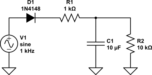
I've been experimenting with a simple rectifier circuit and wanted to share some observations. Without R1, the circuit functions as the well-known half-wave rectifier, where the capacitor quickly charges to the peak voltage of 5−0.7=4.3V, which is intuitive and straightforward to calculate analytically. However, with R1 added, estimating the steady-state capacitor voltage without simulation becomes interestingly challenging.

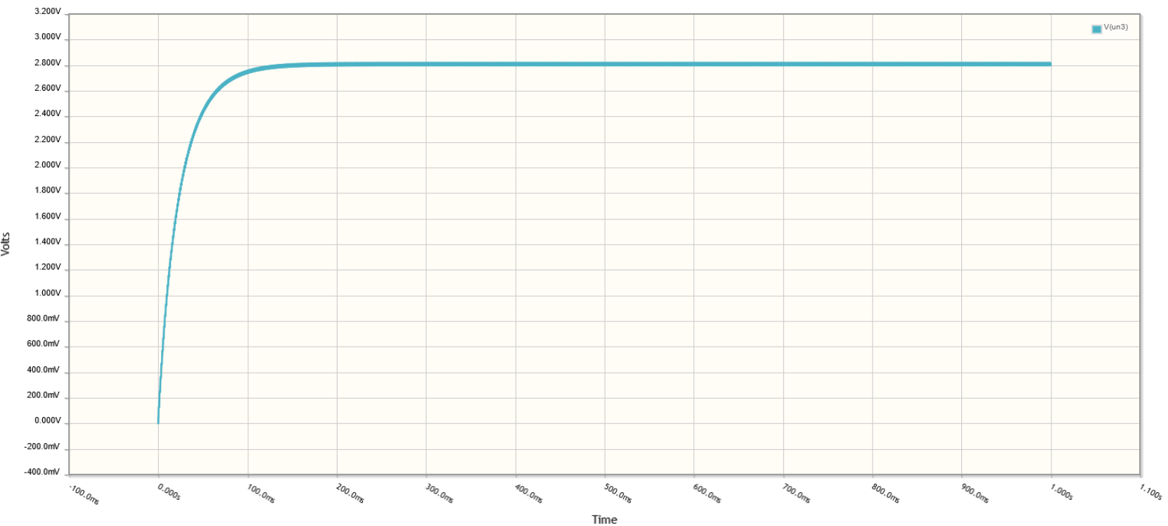
Since the capacitor is relatively large, creating a high RC time constant with R2, it's evident that the voltage across it will stabilize at some DC level (2.8 V in this simulation). Is there an obvious or analytical approach to compute the steady-state capacitor voltage without delving into the diode equation or solving the non-linear circuit equations? Perhaps leveraging the assumption that the capacitor voltage remains relatively constant could simplify things. Am I overlooking something?

The steady-state capacitor voltage should depend on R1, R2, and the peak voltage of the source. However, I haven’t been able to derive a clear expression for it yet.

enter image description here

enter image description here

\$\endgroup\$
3
  • 1
    \$\begingroup\$ I found the reference I mentioned. Chapter 8 of this book seems to cover similar concepts, but it seems to focus more on the opposite situation where the capacitor is in series and diode is the load. The later sections in that chapter cover tubes & transistors with a load capacitor, so you might be able to substitute a diode somehow as the switching element. I haven't really looked at it, but thought it was worth it to share. \$\endgroup\$
    – Ste Kulov
    Commented Dec 3 at 0:47
  • 1
    \$\begingroup\$ Thanks. That's a super interesting and thorough book from the times (60s I believe) when running simulations or building an electronic lab was often impractical or very costly, making analytical methods the norm. It is a like hidden gem. And I think my circuit can still be represented with the diode as the load and the resistor-capacitor network as the source impedance if we take out the diode and find a Thevenin's circuit around it. The same principles in the book can still be applied then. \$\endgroup\$
    – Emin
    Commented Dec 3 at 15:55
  • \$\begingroup\$ If you’re able to apply the info in the book to create a solution, please post your own answer here (you can answer your own question). Then we can vote on it and you can even accept it (put the green checkmark on it). \$\endgroup\$
    – Ste Kulov
    Commented Dec 3 at 21:17

3 Answers 3

2
\$\begingroup\$

This answer might not be what you are expecting, but I think the concept is very useful. It's based on a previous answer of mine found here:

What is the relation between NE555 voltage doubler output voltage vs load?

Note: I would also check out the other answers on this question since it's similar to yours.


Like you said, the circuit is non-linear so it's difficult to come up with an exact answer. However, if you limit the valid range of load resistor values you can use your measurements to calculate a linear equivalent circuit where you can predict the output using a much simpler linear equation. You're basically transforming the non-linear I-V curve of the circuit to a straight-line approximation which crosses two points on the original curve. How good the approximation will be depends on the two points you select, including how close/far-apart they are and also where the points you are trying to predict are in relation to the original two points.

This is basically an application of Thévenin's theorem. You can redraw the circuit to the left of your load resistor as a voltage source and series resistor. You already have one data point from your CircuitLab simulation: (10 kΩ, 2.8 V). In Thévenin applications, it's natural to select the 2nd data point to be when the load resistor is infinite (i.e. open-circuit): (\$\infty\$ Ω, \$V_{th}\$). This allows you to use a simplified version of the Thévenin calculation (shown below) due to the open-circuit voltage being equal to \$V_{th}\$. However, using this data point has some issues for your particular circuit.

$$ R_{th} = R_{L} \cdot \Big( \frac{V_{th}}{V_{out}}-1 \Big) = 10 \text{ kΩ} \cdot \Big( \frac{V_{th}}{2.8 \text{ V}}-1 \Big) $$

First, the infinite load resistance causes the circuit to take a very long time to reach true steady-state. For an ideal diode, \$V_{th}\$ will eventually reach 5V but the 1N4148 simulation model has reverse leakage which will make it reach just shy of 5V (approximately 4.85 V). In real life, your multimeter's input resistance will affect the output measurement even further.

Second, if you picture a diode I-V curve, the current hangs near zero for a very wide range of low voltages. The infinite load resistance means you're taking the data point at the origin. So a linear approximation (red) made from one point at the origin and one point elsewhere on the original curve (green) will look something like below. As you can see, this is a very poor approximation.
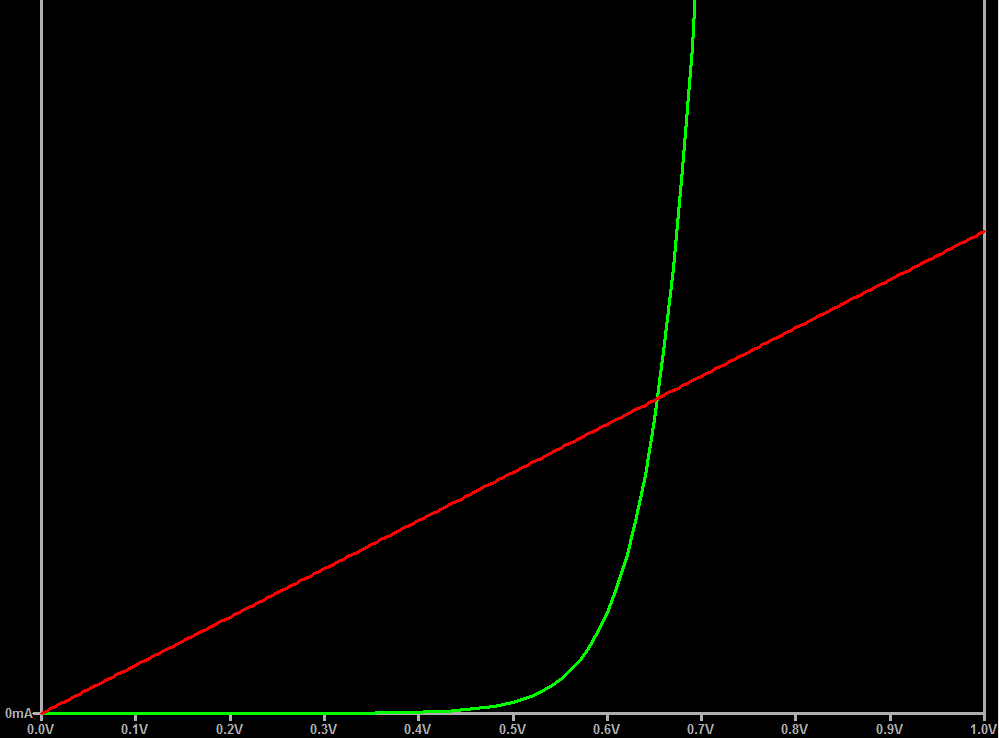
poor I-V curve approximation


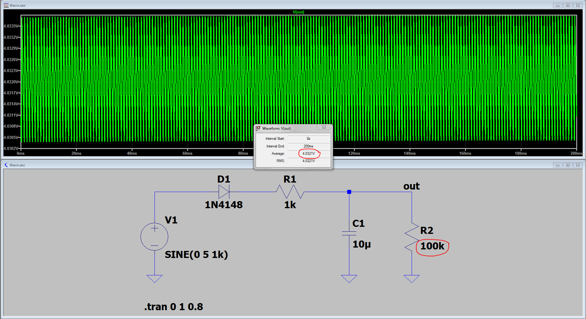
Therefore, you need to pick a more practical 2nd data point for this kind of circuit. Let's choose 100 kΩ. Simulating both 10 kΩ and 100 kΩ loads, we get the following data points for \$(R_{Lx},V_{outx})\$:

$$ \begin{align*} (R_{L1},V_{out1}) &= (10 \text{ kΩ},2.816 \text{ V}) \\ (R_{L2},V_{out2}) &= (100 \text{ kΩ},4.032 \text{ V}) \end{align*} $$
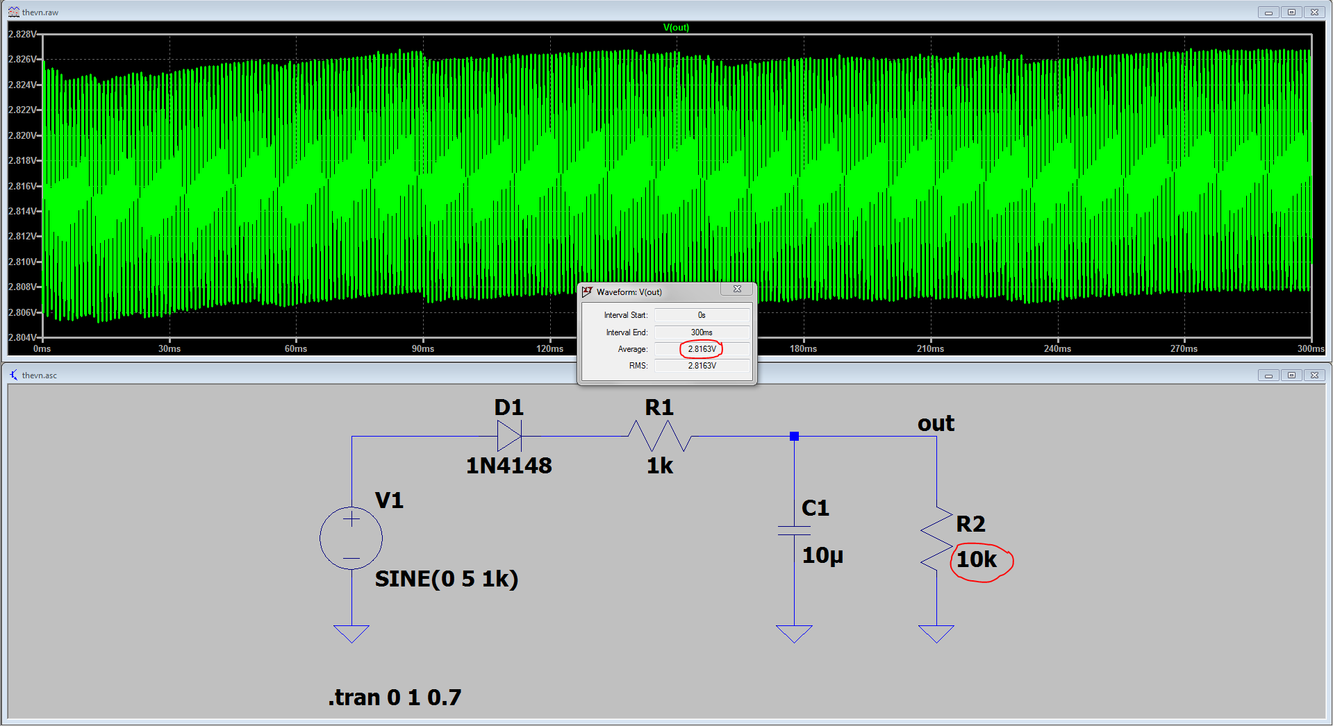
voltage for 10k load

voltage for 100k load


Using the equations from the answer I linked above, we can calculate \$R_{th}\$ and \$V_{th}\$ from these two data points.

$$ \begin{align*} R_{th} &= \frac{R_{L1}R_{L2}(V_{out2} - V_{out1})}{V_{out1}R_{L2} - V_{out2}R_{L1}} \\~\\ R_{th} &\approx 5.040 \text{ kΩ} \\~\\ \\ V_{th} &= V_{outx} \cdot \frac{R_{th} + R_{Lx}}{R_{Lx}} \quad \text{for} \ x = 1 \ \text{or} \ 2 \\~\\ V_{th} &\approx 4.235 \text{ V} \end{align*} $$

We can now compare our linearized circuit with the actual circuit and see how well our approximation does. First, we start with the points we used to construct the approximation. If we didn't make a mistake in the calculations, the approximation should match up exactly with the original circuit for 10 kΩ and 100 kΩ loads...and they do.
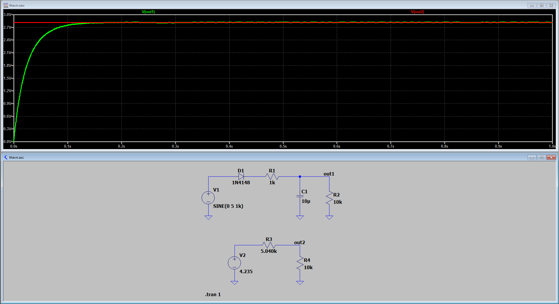
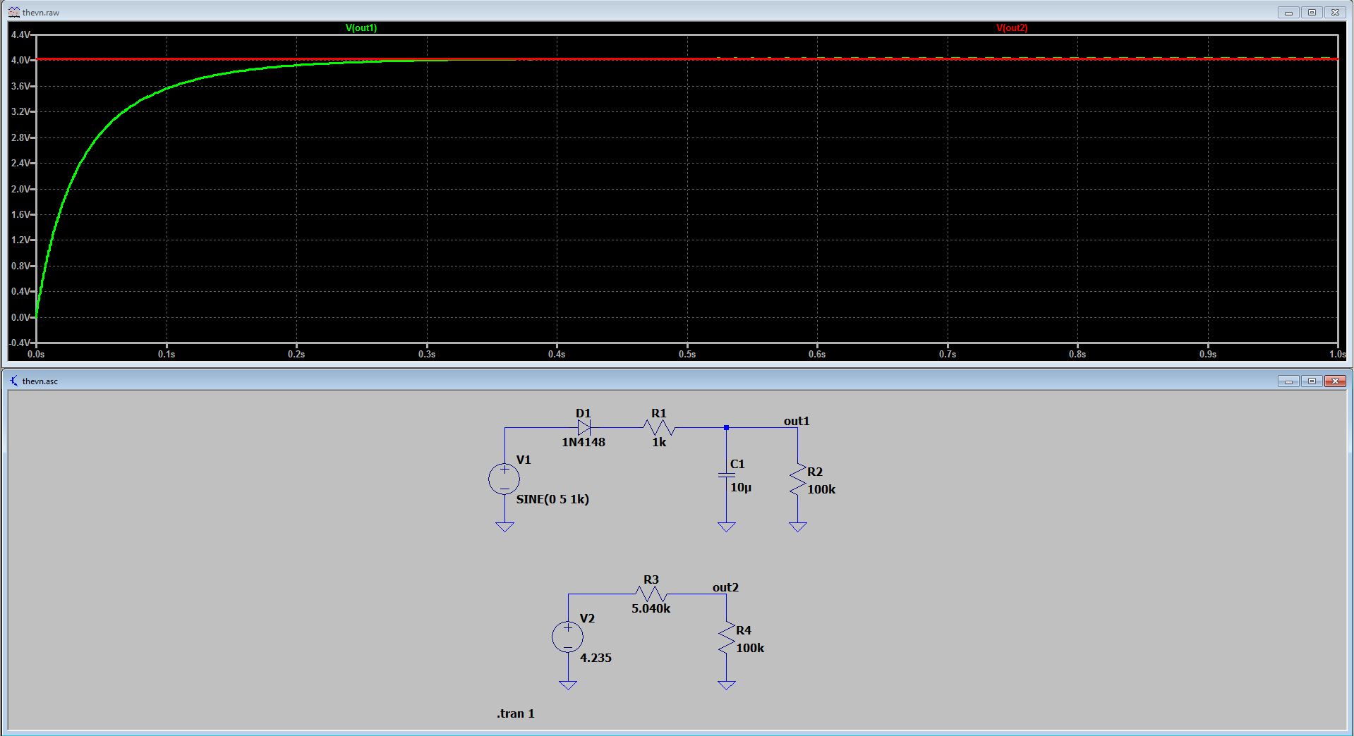
10k load comparison

100k load comparison


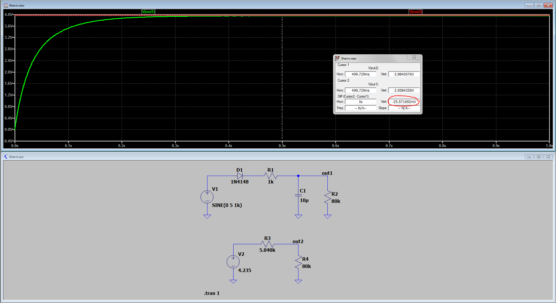
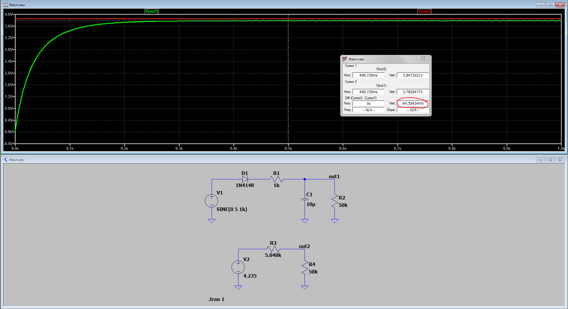
We can try some points in between to see how well the approximation fares. Let's try 20 kΩ, 50 kΩ, and 80 kΩ. I circled the voltage difference between the original and the approximation in red.
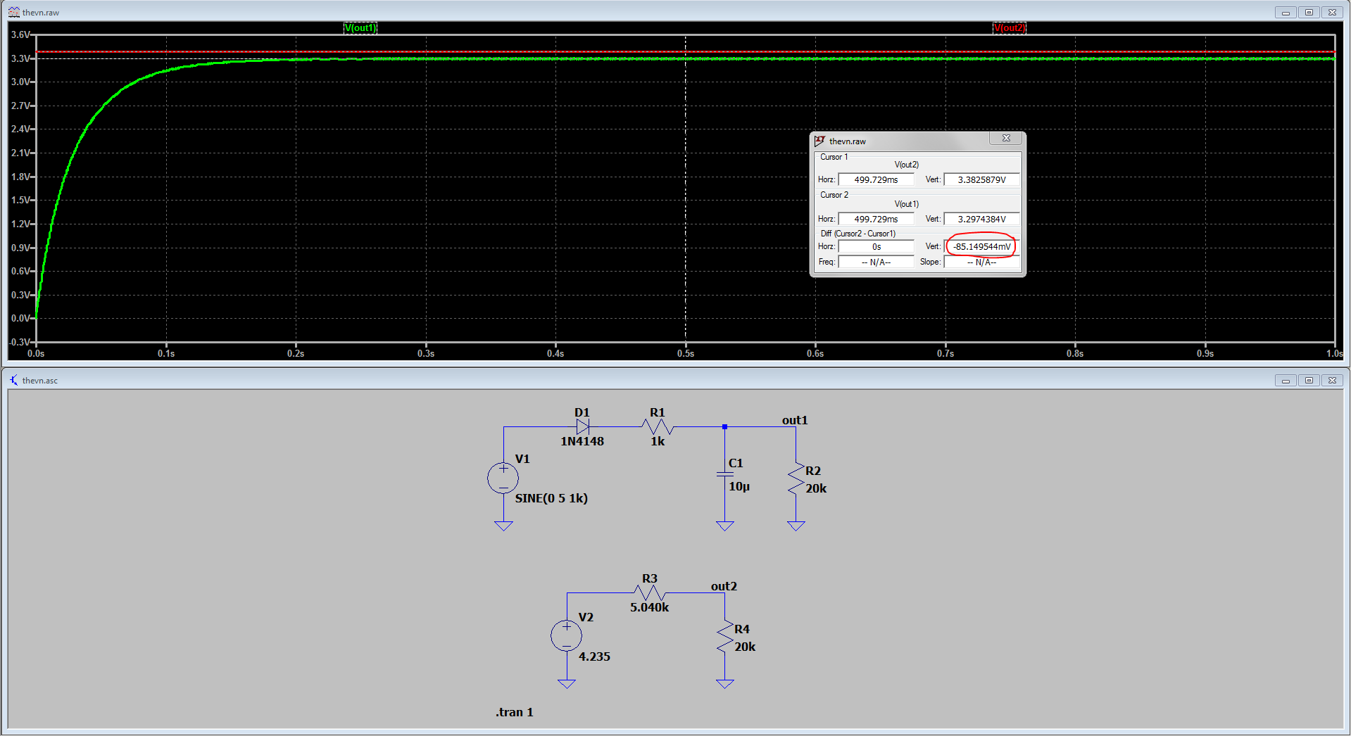
20k load comparison

50k load comparison

80k load comparison


That's pretty darn close. OK, so let's try some points outside the original range of 10 kΩ to 100 kΩ. How about 5 kΩ and 200 kΩ?
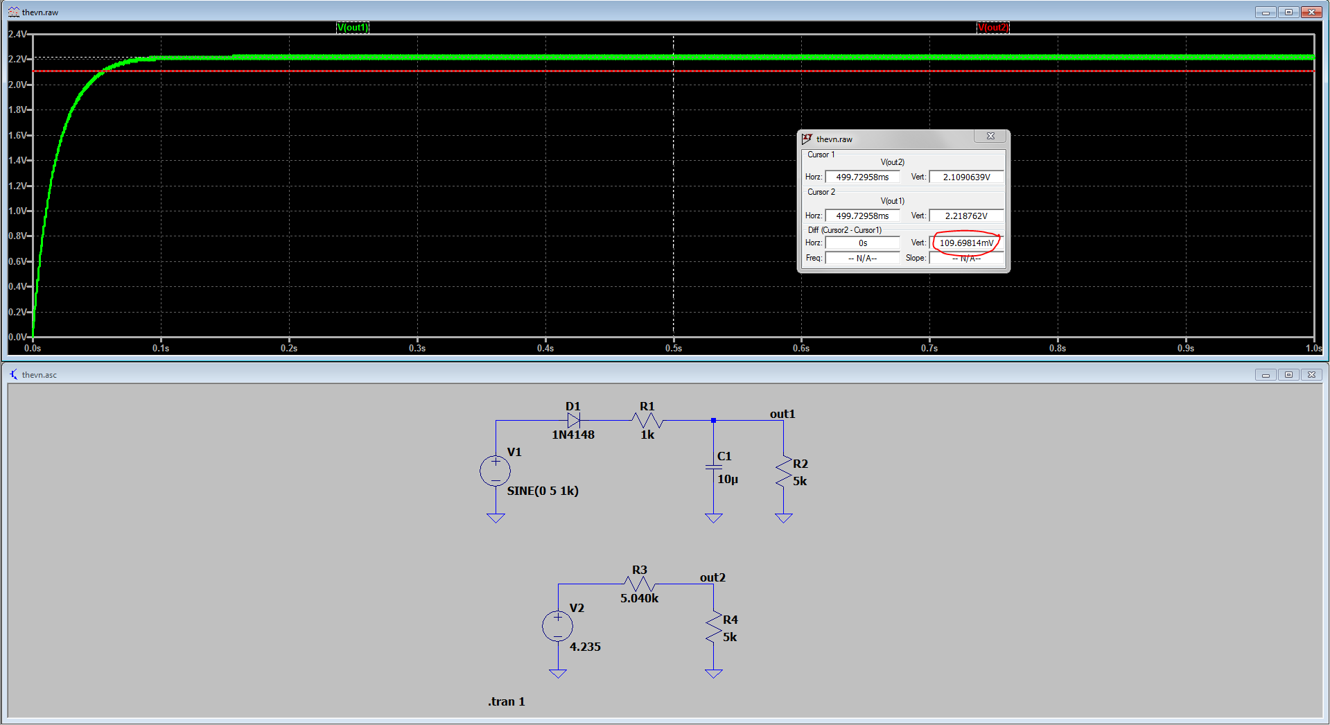
5k load comparison

200k load comparison


A little bit worse, but still really good. OK, so this approximation can work for us reasonably well under these load conditions. So how do we use it without the simulator? Well, a Thévenin equivalent connected into a load resistor is just a simple voltage divider circuit. So for this particular circuit, we can approximate the output voltage \$V_{out}\$ given the load resistance \$R_{L}\$ as such:

$$ V_{out} \approx 4.235 \text{ V} \cdot \frac{R_L}{5.040 \text{ kΩ} + R_L} $$

For example, for \$R_L = 68 \text{ kΩ}\$ we should get:

$$ V_{out} \approx 4.235 \text{ V} \cdot \frac{68 \text{ kΩ}}{5.040 \text{ kΩ} + 68 \text{ kΩ}} \approx 3.943 \text{ V} $$


This technique can be very useful if utilized properly while understanding its limitations. The better you can place your two data points with respect to your intended operating condition range will determine how accurate your approximation can be over that range. In the real world, you can use this scheme to measure and characterize unknown circuits, such as the output pin of an integrated circuit. Take two load resistor measurements on the bench which you can then use to construct a fairly reasonable approximation (in many cases). See the answer I linked above for more details.


One last thing to mention for completeness. If you know your calculus, a straight line intersecting a function at two points is known as a secant line. As these points move closer together such that they are almost on top of each other results in what we call a tangent line. You can apply a similar concept here. If you need a really good approximation for a 10kΩ load (not a range), you can pick the 10 kΩ point and something like a 10.1 kΩ point for your calculations. Then the resulting approximation will be very good around 10kΩ, but nowhere else. The limiting factor for this kind of calculation will depend on how good the SNR and precision are for your measurement equipment. If the resulting measured voltage for the 10.1 kΩ load is not much different than the 10 kΩ load, then you might need to try something like 10.5 kΩ or 11.0 kΩ.

\$\endgroup\$
3
  • 1
    \$\begingroup\$ Thanks. This is a very powerful technique that can come in handy in practice when you can actually take measurements and you need a linear approximation of one part of the circuit. I was hoping more for a pen and paper analytical solution in case you don't have the means to simulate or measure the circuit. However, this appears to be much more challenging to do than it initially seems, even after the fact that we know that the capacitor voltage will stabilize at some DC level. I'll also make sure to read the answers in the other question you linked. \$\endgroup\$
    – Emin
    Commented Dec 2 at 16:49
  • \$\begingroup\$ @Emin Yep. I use this quite frequently in practice. I knew it wasn’t what you were looking for, but thought it could be of use. Keep in mind that your pen and paper calc for the open circuit voltage assuming the diode had a 0.7V drop was incorrect in this instance. So those kinds of approximations have limitations too. I seem to recall an old book I had which had approx calculations for diode + capacitor charging/discharging circuits. But it might only work for pulse/square waves and not sine waves. Anyway, if I find it and it applies here I’ll let you know! \$\endgroup\$
    – Ste Kulov
    Commented Dec 2 at 22:56
  • \$\begingroup\$ @Emin I just realized I misinterpreted the text in your original question. I thought you said R2 was removed when you got 4.3V, but you said when R1 is shorted is when you got 4.3V. I rewrote the answer a bit to reflect this. My overall point in the above comment still stands, since in the "half-wave rectifier" circuit you get 4.3V only with a 10kΩ load. This incorrectly makes you think the constant "0.7V silicon diode voltage drop" pen and paper approximation holds quite well, but if you adjust the load resistor from 10kΩ to 1kΩ you now get 4.09V (i.e. 0.91V drop across the diode). \$\endgroup\$
    – Ste Kulov
    Commented yesterday
1
\$\begingroup\$

There is an analytical approach, but it is not simple.

The capacitor voltage will stabilize at a value for which the charge into the capacitor during a cycle equals the charge out. This is complicated by the fact that the charging/discharging duty cycle and the magnitudes of the charge and discharge currents are all functions of the actual capacitor voltage, which generally means that the final equation you need to solve will be a nonlinear one. It might not even have a closed-form solution, which would mean that getting an answer will require numerical methods — which is essentially what your simulation is doing.

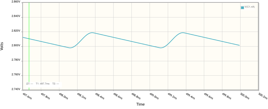
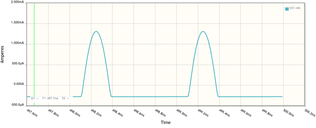
To get a sense of this, plot the capacitor current in your simulation. Zoom in on the time scale until you can see one or two cycles at a time. You'll find that the waveform at the end of the simulation has equal areas on the positive and negative sides. The shape of the wave on either side will give you a feel for the difficulties involved with coming up with an analytical solution — the charging pulse is a small portion of the sine wave, while the discharging pulse is a slow exponential curve (very nearly linear).

schematic

simulate this circuit – Schematic created using CircuitLab

voltage waveform

current waveform

\$\endgroup\$
1
  • 1
    \$\begingroup\$ This is what I realized too. I even tried to obtain an equation (non-linear or approximately linear) for the on/off times of the diode (\$t_{ON}\$ and \$t_{OFF}\$) using the capacitor charge/discharge balance and \$t_{ON}+t_{OFF}=1ms\$ to form two equations and two unknowns. However, the sinusoidal input voltage introduces complexity compared to the switched waveforms typically seen in power electronics circuits. I was hopeful there might be a straightforward way to calculate this voltage using basic circuit techniques and algebra, but it seems to be more involved than that. \$\endgroup\$
    – Emin
    Commented Dec 2 at 15:48
1
\$\begingroup\$

Update:
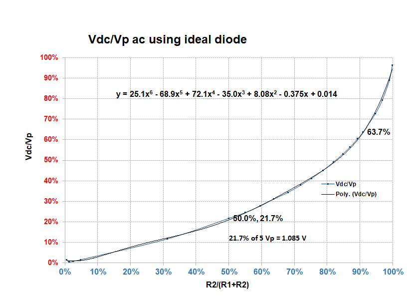
There is no simple formula for the Vdc out as this is a nonlinear circuit. I recall our Hammond power supply designer circa the mid-80s having elegant nomographs for all these and similar types of nonlinear equations in his textbook. I can't do the same, but I simulated it in Falstad using a 1N4148 and then an ideal 0V diode. Then, I plotted it in a spreadsheet to find the nonlinear effect of the diode-drop Vf an enigma as well as the Vcap variations.

  1. With R1=0, Vcap follows the source peak minus the diode drop, \$V_{cap} = V_p - V_f\$
  2. For a full-wave rectifier it is the same voltage with R=0 and no load. Still, with a large series R and C shunt filter, we see an average with the diode conducting for only a tiny duration at the peak just enough to supply the diode reverse leakage current so the Vf drop of say 300 to 400 mV has no effect on the no-load voltage but will affect duty factor and Vf with a load. With Vf and If and the phase angle of diode conduction with a sine voltage we now have 6 unknowns and at best 4 equations.
    \$V_{avg}= \frac{2}{\pi}Vp\$
  3. But with a half-wave and a load R the steady-state Vcap reduces with an average pulsed-sine current from the diode and a bit more than a half-wave of steady DC-current from Vcap.
  4. The diode current for Vf depends on the size of the current rating and the load of (Vpk-Vout)/R1. But Vout also depends on the discharge current of Vout/R2. Since the current duty factor changes rapidly with rising R1. Then the effect of diode drop is attenuated rapidly from lower current.
  5. The result is a 6th order equation.

10 uF at 1 kHz \$Z_c=2π(1000)(10×10−6)1​≈15.92Ω\$ thus compared to 10K shunt we can neglect Vac ripple.

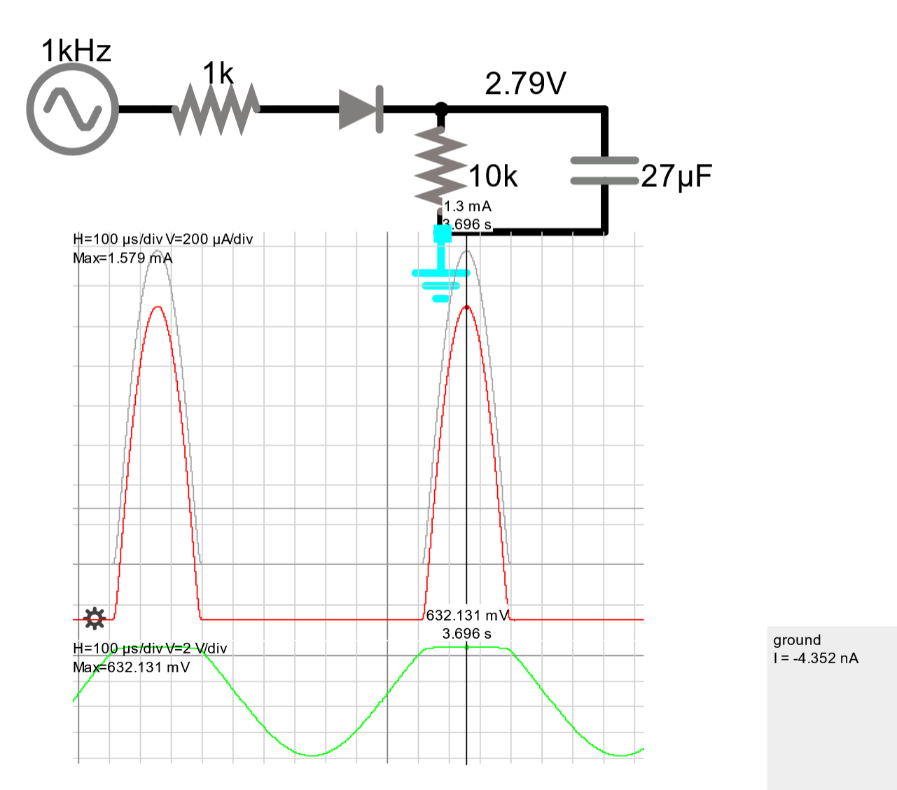
I assume that for < 5 mA max and > 1 mA min the diode drop will be closer to 650 mV but with no load Vf drops to Vf= 253 mV with a peak current of 614 nA from diode leakage.

With R1=1k, R2=10k, R1/(R1+R2)= 90.9%, reducing an ideal rectifier Vcap from 100% to 63.7% of 5V = 3.18 V.

With Vcap=2.79V, the diode peak was Vf =632 mV max with a difference of 3.18-2.79= 390 mV due to the average rise in diode Vf effect vs an ideal of 0 mV.

Conclusion
This non-linear simple circuit, teaches us not to assume linear KVL will work for diodes when averaging with high series and shunt R's with a half-wave and storage cap.

enter image description here enter image description here

end update


R1 & R2 still limit the current after the cap is charged up thus if we can integrate the partial peak sine.

If both R values were equal and we average Vout instead of half of 50%=R2/(R1+R2) being 25% of 4.35V = 1.09V we will get less. This is because the diode connects much less than half the time as the cap being charged near 1V only conducts in between 1V and 4.35 V or 1/3 of the time.

So interpolating between equal R1/R2= 50% and 0% the voltage ranges from 1 to 4.3V. So my quick estimate is for R1/R10=10% is Vout will be (1-10%) of 4.3V = 3.87 V.

(nice try but no cigar)

\$\endgroup\$
1
  • 1
    \$\begingroup\$ The capacitor voltage stabilizes at 2.8 V when R1 = 1 kΩ and R2 = 10 kΩ. I was hoping to estimate this value using just the resistor values or ratios, along with the diode's forward voltage drop and the source's peak voltage. However, it turns out to be surprisingly difficult to calculate analytically. While you can narrow down a range of possible values using some insights, adding R1 to the current path significantly complicates finding an exact value, even though the final capacitor voltage is constant at the end of the day. \$\endgroup\$
    – Emin
    Commented Dec 2 at 15:58

Your Answer

By clicking “Post Your Answer”, you agree to our terms of service and acknowledge you have read our privacy policy.

Not the answer you're looking for? Browse other questions tagged or ask your own question.