12
\$\begingroup\$

I am trying to design a BJT amplifier following this model: enter image description here
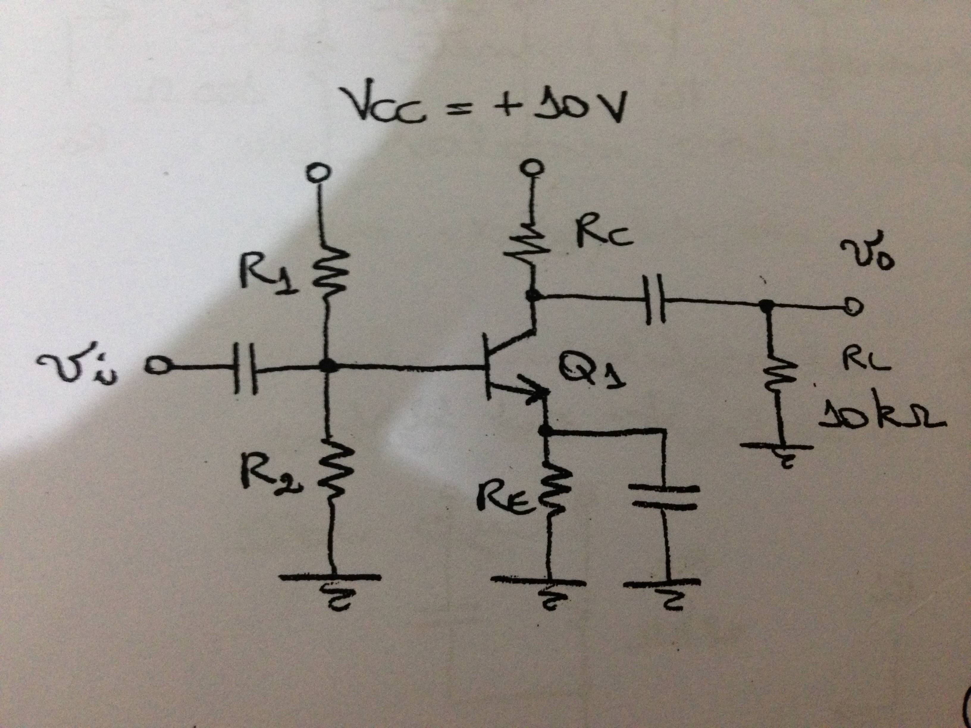
Where the beta parameter may vary from 100 to 800, the voltage between the base and the emitter equals 0.6V (active mode), \$V_t = 25 mV\$ and the Early Effect may be ignored.

It can also be supposed that the bypass capacitors simply act as a short circuit for AC and open circuit for DC.

There are three constraints:

  • Static Power Dissipation < 25mW;
  • Output Signal Swing of 6Vpp
  • Maximum error of 5% at the collector current for any variation at beta

I've been able to show that the voltage between the collector and the emitter will be 3.2V (using the signal swing information), but I don't know what to do next.

Edit:

Calculation that led to \$V_{CE} = 3.2V\$:

The output signal swing yields that the upper limit will be +3V and the lower limit will be -3V. The amplifier will either cutoff or saturate. Also, the circuit is a linear system which means that the Superposition Theorem may be used. At any node, the voltage will be the sum of the polarization (DC) voltage and the signal (AC) voltage. So, using the signal swing and supposing symmetrical output (\$V_C\$ and \$V_E\$ are the polarization voltages at the colletor and emitter):

\$V_{cmax} = V_C + 3V = V_C + v_{omax} = V_C + I_C * R_C//R_L\\ V_{cmin} = V_C - 3V\$

The first equation says that \$ I_C * R_C//R_L = 3V\$ (cutoff condition, no current entering the transistor; \$i_{R_C} = i_{R_L}\$) and operating with the second equation (supposing that the minimum collector voltage is \$V_E + 0.2V\$ which leads to saturation):

\$V_{cmin} = V_C - 3V = V_E + 0.2V \rightarrow V_C - V_E = 3V + 0.2V \rightarrow V_{CE} = 3.2V\$

\$\endgroup\$
4
  • 2
    \$\begingroup\$ Next, you simulate the thing and play with part values until you get the behavior you want. \$\endgroup\$
    – Kaz
    Commented Sep 22, 2013 at 2:41
  • 3
    \$\begingroup\$ Didn't your instructor provide some equations and a procedure for solving this? Is there some conceptual issue you are struggling with? \$\endgroup\$
    – Joe Hass
    Commented Sep 22, 2013 at 12:42
  • \$\begingroup\$ Show the calculation which led to \$V_{CE}=3.2V\$ please. \$\endgroup\$
    – Vasiliy
    Commented Sep 22, 2013 at 13:11
  • \$\begingroup\$ Added the calculation for \$V_{CE} = 3.2V\$. My instructor did provide the equations and the models used to analyze transistor circuits, but not exactly how to solve such a problem. I'm not supposed to simulate it. \$\endgroup\$
    – Thiago
    Commented Sep 22, 2013 at 16:18

2 Answers 2

6
\$\begingroup\$

First, translate the specifications into constraint equations.

For the static power dissipation:

Assume, for now, that \$I_{R2} \ge 10 \cdot I_B = \dfrac{I_C}{10}\$ for the worst case \$\beta = 100 \$.

The supply current is then:

\$I_{PS} = I_C + 11 \cdot I_B = 1.11 \cdot I_C \$

The static power constraint then becomes:

\$\rightarrow I_C < \dfrac{25mW}{1.11 \cdot 10V} = 2.25mA\$

The bias equation:

The BJT bias equation is:

\$I_C = \dfrac{V_{BB} - V_{EE} - V_{BE}}{\frac{R_{BB}}{\beta} + \frac{R_{EE}}{\alpha}} \$

For this circuit, we have:

\$V_{BB} = 10V \dfrac{R_2}{R_1 + R_2}\$

\$V_{EE} = 0V\$

\$V_{BE} = 0.6V\$

\$R_{BB} = R_1||R_2\$

\$R_{EE} = R_E\$

So, the bias equation for this circuit is:

\$I_C = \dfrac{10V \frac{R_2}{R_1 + R_2} - 0.6V}{\frac{R_1||R_2}{\beta} + \frac{R_E}{\alpha}} \$

Now, you want less than 5% variation in \$I_C\$ for \$100 \le \beta \le 800\$. After a bit of algebra, find that this requires:

\$ \rightarrow R_E > 0.165 \cdot R_1||R_2 \$

Output swing:

The positive clipping level can be shown to be:

\$v^+_O = 3V = I_C \cdot R_C||R_L \$

The negative clipping level can be shown to be about:

\$v^-_O = -3V = I_C(R_C + R_E) - 9.8V \rightarrow 6.8V = I_C(R_E + R_C)\$

Put all this together:

Choose, for example, \$I_C = 1mA \$ then:

\$R_C||10k\Omega = 3k\Omega \rightarrow R_C = 4.3k\Omega\$

\$R_E + R_C = 6.8k\Omega \rightarrow R_E = 2.5k\Omega \$

Thus, \$V_E = 2.5V\$ and \$V_B = 3.1V\$

Then,

\$R_2 = \dfrac{V_B}{10 \cdot I_B} = \dfrac{3.1V}{100\mu A} = 31k\Omega \$

\$R_1 = \dfrac{10 - V_B}{11 \cdot I_B} = \dfrac{6.9}{110\mu A} = 62.7k\Omega \$

Now, check

\$0.165 \cdot R_1||R_2 = 3.42k \Omega > R_E \$

So, this doesn't meet the bias stability constraint equation we established earlier.

So run through this again (use a spreadsheet!) with larger \$I_C\$ until you've met the bias stability constraint equation.

If you can't meet the constraint with \$I_C < 2.25mA \$, you may need to increase current through the base voltage divider, e.g., \$I_{R2} = 20 \cdot I_B \$ and work through the static power constraint again.


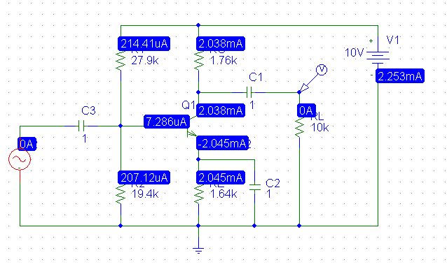
As the the correctness of the clipping level calculations above has been questioned, I simulated the circuit using values calculated from the above except that \$I_C \$ was increased to \$2mA\$ for the calculation.

The DC solution:

enter image description here

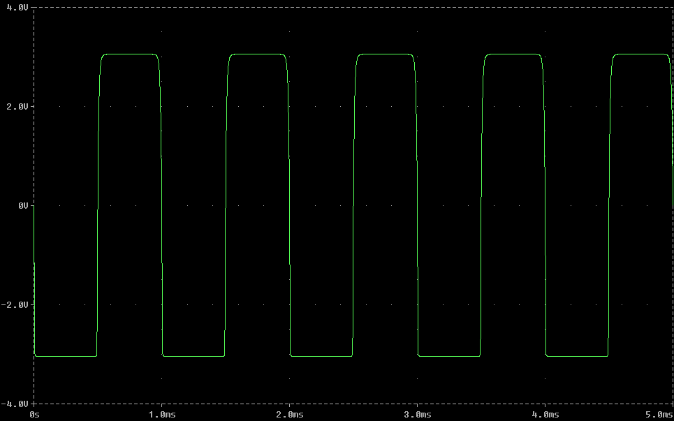
Driving the amplifier with a 500mV 1kHz sine wave:

enter image description here

Note the clipping levels are precisely +3V and -3V as designed. The variation in \$I_C\$ is just over 5% over the range of \$\beta\$ so the next step would be to increase the multiple of base current through R2 to e.g., 20 and plug in the numbers (which does result in meeting all the constraints).

\$\endgroup\$
5
  • \$\begingroup\$ I think that \$R_E\$ should not appear in the equation for negative clipping since it is completely bypassed by the capacitor. In the reference you provided the battery does replace the capacitor, but the presence of \$R_3\$ is not analogous to OP's circuit. \$\endgroup\$
    – Vasiliy
    Commented Sep 22, 2013 at 20:39
  • \$\begingroup\$ @Vasiliy, \$R_E \$ must appear in the equation since the voltage across the emitter bypass capacitor is precisely \$I_E R_E \$. \$\endgroup\$ Commented Sep 22, 2013 at 20:55
  • \$\begingroup\$ DC voltage yes, but regarding voltage swing you mean AC voltages, no? \$\endgroup\$
    – Vasiliy
    Commented Sep 22, 2013 at 20:59
  • \$\begingroup\$ @Vasily, the linked document on clipping levels is quite straightforward. Setting R3 to zero, it is clear that the most negative clipping voltage across the load is precisely: \$v^-_O = (I_E R_E) + V_{CEsat} - (V^+ - I_C R_C)\$ The first term on the right is the DC voltage across the emitter bypass capacitor. The last term on the right is the DC voltage across the output coupling capacitor. For clipping level calculations, it is assumed that the coupling capacitors can be replaced by batteries, i.e., that they are AC short circuits with a DC voltage across. \$\endgroup\$ Commented Sep 22, 2013 at 21:21
  • \$\begingroup\$ I'm missing your point. I'll try to read this again later - maybe then I'll understand. Thx \$\endgroup\$
    – Vasiliy
    Commented Sep 22, 2013 at 21:54
6
\$\begingroup\$

Since this is an academical task, let me give you some guidance rather than a complete answer.

The amplifier in question is common-emitter amplifier. You can find a short overview and basic equations for this amplifier here.

Now, let's see what should you look for in order to satisfy all the constraints.

Static power dissipation:

The whole purpose of resistors \$R_1\$ and \$R_2\$ is to provide voltage and current biases to the base of BJT. Their value should be taken as high as possible in order to minimize static power consumption and increase amp's input impedance. However, in order for the voltage at base terminal to be stable at the value imposed by this divider, the following condition must be satisfied:

$$(\beta +1)R_E >> R_1||R_2$$

If the above constraint is satisfied, you know the value of the voltage at base terminal. Calculating emitter's voltage is straightforward.

The values of these resistors will sometimes be high enough for the static power drawn by this voltage divider to be negligible. I believe that this condition holds in this configuration, though if you make this assumption you must check its validity after you solve the question.

Additional DC current path is:

$$power supply \rightarrow R_C \rightarrow Q_1 \rightarrow R_E \rightarrow gnd$$

You need to calculate the DC current in this path and use a standard \$P=IV\$ equation in order to express the static power in this branch as function of \$R_C\$ and \$R_E\$.

Add the two contributions together.

Output voltage swing:

You must ensure that the output voltage can oscillate 6Vpp. The most straightforward constraints on collector's DC voltage following from this requirement are:

$$V_C>V_{E}+V_{BE}+\frac{Vpp}{2}$$

$$and$$

$$V_C<V_{CC}-\frac{Vpp}{2}$$

Note that the transistor can't be in cut-off in this configuration as \$V_{BE}\$ is constant (due to the presence of bypass cap).

Also, usually, you want to avoid \$V_{CE}\$ to go too low so that the transistor will enter saturation. Entering saturation causing a serious distortion of the output signal. Though you can ignore this constraint if you haven't learned this yet.

AC collector current as a function of \$\beta\$:

Draw the small signal model of the amplifier and obtain the equation which relates collector's current with all the relevant parameters of the problem. Check for the parameters which can minimize the error due to variation in \$\beta\$.

Honestly, my intuition says that this is impossible - x8 variation in \$\beta\$ seems too high for 5% variation in collector's AC current. Can it be the case that the current in question is DC one?

Summary:

This is very interesting and complex problem. I'm not sure that there is an analytical method which allows to satisfy all the constraints altogether. Start by satisfying them one after another, and get back and change parameters when you encounter a dead end. I believe you'll be done after 2-3 iterations though I did not solve the question myself.

Good luck

\$\endgroup\$
1
  • \$\begingroup\$ @Vasily, the constraint is on variation of the DC collector current. \$\endgroup\$ Commented Sep 22, 2013 at 20:58

Your Answer

By clicking “Post Your Answer”, you agree to our terms of service and acknowledge you have read our privacy policy.

Not the answer you're looking for? Browse other questions tagged or ask your own question.