**EOS/ESD prevention Experience**
The reason for the acceptable range of 1M to 10 M is to current limit static discharge for wrist straps.
- It does this by bleeding body charge slowly to the same potential of the case or gnd reference that the 1M resistor is clamped to, while static charge may be generated by motion or change in body capacitance with a fixed charge, V=C/Q .
> - Thus for example, consider a 10000 pf body surface to stray air charged at 10kV then connected to a 1M current limiting resistor, we might expect 10k/1M or 10mA with a decay time of 1M*10nF=10ms which is faster than pre-ionization time, so the resistor might be bypassed. But with it connected all the time, the rate of charge build up dV/dt is much slower than the discharge time so body charge levels are kept at relatively low levels.
- meanwhile the finger tip model of 100-300pF * 1M = 100u-300us decay time keeps fingers with wrist straps to ground discharged faster from tribe-electric effects and thus momentary charge build up of 1kV is limited to 1mA.
> to verify this understanding yourself, recall the current zap you heard with a key or finger to metal ESD discharge and compare your experience touching a grounded tree (not paint or plastic) due to surface resistance, you likely would not feel anything and yet this can be enough to damage unprotected microwave FETs with 25V BDV, but your experience tells you the series surface resistance limited the current.
For Electrostatic Over Stress or EOS prevention all surfaces must be "Static Dissipative" to prevent rapid discharge.
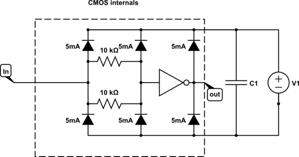
The other reason is to reduce the potential ionization discharge time from 5-100 picoseconds that creates E-Field transients faster than the ESD diodes can response when CMOS inputs are connected to long cables (antenna).
<!-- Begin schematic: In order to preserve an editable schematic, please
don't edit this section directly.
Click the "edit" link below the image in the preview instead. -->

<!-- End schematic -->
For the same reasons flooring and work surfaces need to \$10^{10}\$ Ohms per square.
- It is well known that e-field discharges in one place may conduct via a long ground path and radiate from this path to damage very sensitive parts from the resulting antenna efficiency of interconnects to sensitive parts at frequencies dependant on the rise time of the discharge.
- I have seen photos and many journal researchers validate that finger ESD may have a current transition time down to 5-10ps which has been captured. This translates to a continuous Fourier Spectrum of at least f=1/3t or roughly 25-50GHz which has a corresponding very short wavelength at the upper range.
> So effectively any length can capture some of the transient Field and thus is EOS unsafe. We rate parts only with 100pF or 300F for Human finger capacitance due to the tiny area of contact. But in reality, between two hands we can measure with an RLC meter and "good contact area" with probes 100x more capacitance easily. Thus ESD generated by walking on dry dusty floors or hotel nylon carpets with key can generate a healthy arc of 30kV or ~3cm and a good zap and radiate within the entire room. Due to RF properties & physics, one cannot guarantee to zap any unprotected Semi, nor can you guarantee that it is not "wounded" a similar breakdown ratio in kV/mm now attenuated to small levels and distances but only slightly higher ratios of mV/nm in charged dielectric junction BreakDown Voltages (BDV) spanning xx nm.
> This is also a future limitation for Moore's Law Lithography shrinkage in CPU's. If the junctions got much smaller, it can approach BDV levels of Silicon in xx mV/nm ratings.
> - It is also a huge challenge for semiconductor Prcoess Engineers to avoid ESD in the fabrication of semiconductors with triboelectrically charged material e.g. Silicon and Gallium Arsenside vapours superheated being deposited on junctions
- A risky but effective alternative when a wrist strap is not available, is to be aware of triboelectric surfaces , discharge surfaces and all static sensitive devices and touch fingers while holding a PCB ground tab before handing it to the other person.
- OR, always keep one finger at least on a PC case so to remain at the same E field strength as the PCB inside grounded to the case, when changing parts.
- OR to gently touch a grounded surface away with your 1M "calibrated" finger tip (using DMM or RLC) and don't touch your breadboard before doing this, then be aware how easy E fields can be created.
- In my past 40 yrs experience before I implemented EOS prevention in the electronics factory, I can tell you how easy it was to reset a Motorola Emulator or an Apple ][ just from ESD 10m away. The lab was surrounded by a grounded cage (antenna) and at time in the 80's nylon commercial carpet made great ESD generators with neoprene soled shoes. (salty leather is better)
Most MOBO's use insulated standoffs, and a few use conductive, so Ground connection is thru DC plug to ATX PSU to case ground, where ground is local reference to case. WHen connected to Power outlet, the local case ground is connected to earth ground thru household wiring, but very inductive , so the case is the best shield.
( except for long IO cables , special case beware they can carry ESD charges from tribo-electric friction)
**- example** When I was TE Mgr, technicians would drag 10m SCSI cables on dry concrete floor ( with dust) and connect to towers in Final Test and blow SCSI drivers from ESD, until we trained them to touch Connector shell and frame before connection.