Having solved the mystery of ["pulling" and "pushing" devices](https://electronics.stackexchange.com/q/664001/61398), it would be interesting to do the same with "sourcing" and "sinking" devices.
Background
=======
A transistor with a constant base-emitter voltage represents a *constant current source* (to be more precise, we should also include the power source).
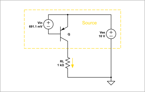
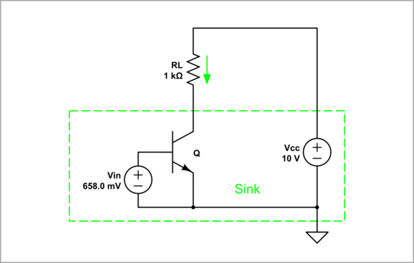
For example, in the CircuitLab schematics below, I have adjusted the base-emitter voltage so that to pass 1 mA current through the load. If you want to change it, open Vin's *parameters* window, hover the mouse over RL, and adjust Vin while looking at the reading. If the *parameters* window covers RL, then move the schematic to the right edge of the screen, open and click on *parameters* to pin it, and return the schematic to the left side of the screen.
Note something interesting in this arrangement - the collector and emitter currents are equal because the base current is not added to the emitter one.
Varieties
======
Depending on the place of insertion, we call this device by different names.
"Current source"
--------------
If we connect the transistor Q with its emitter to the positive supply rail, and the load RL to ground, we call it "current source".
<!-- Begin schematic: In order to preserve an editable schematic, please
don't edit this section directly.
Click the "edit" link below the image in the preview instead. -->

<!-- End schematic -->
"Current sink"
--------------
If we connect an NPN transistor Q with its emitter to ground, and the load RL to Vcc, we call it "current sink".
<!-- Begin schematic: In order to preserve an editable schematic, please
don't edit this section directly.
Click the "edit" link below the image in the preview instead. -->

<!-- End schematic -->
Both?
-----
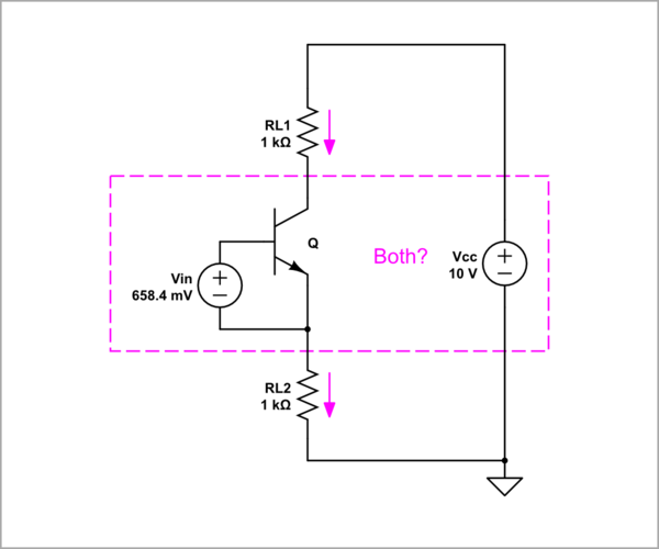
But what should we call (what is) the transistor when it is "floating" between two loads RL1 and RL2?
<!-- Begin schematic: In order to preserve an editable schematic, please
don't edit this section directly.
Click the "edit" link below the image in the preview instead. -->

<!-- End schematic -->