Start with the speaker itself. You want to drive it, somehow.
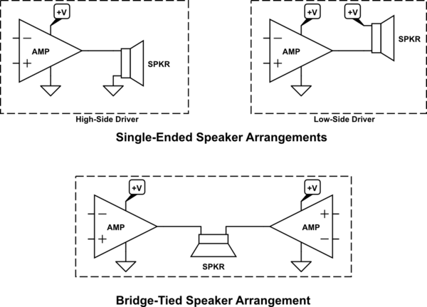
So, here are three different, but relatively common arrangements to consider with a semiconductor driver circuit that is powered by a single supply rail. (There are others, such as ones using an audio transformer.)
<!-- Begin schematic: In order to preserve an editable schematic, please
don't edit this section directly.
Click the "edit" link below the image in the preview instead. -->
<!-- End schematic -->
The ideas are pretty simple. The two single-ended cases share a common power supply rail with the speaker and directly driving only one end of the speaker. Hence, *single-ended*. The bridge-tied load arrangement places the speaker in between two amplifiers that are \$180^\circ\$ out of phase with each other (when one is driving the voltage upwards, the other one is driving the voltage downwards.) (I've shown the amplifiers with the + and - terminals inverted relative to each other to point up the phase difference.)
The bridge-tied load is often used when you can afford to use two amplifiers because it allows you to get the most power delivered to a given speaker when using a single power supply. (Better quality commercial amplifiers will often allow themselves to work correctly in this mode.) For ICs, the TDA8551 is an example of a bridge-tied amplifier that can deliver \$1\:\textrm{W}\$ into an \$8\:\Omega\$ speaker when running from a single \$+5\:\textrm{V}\$ voltage rail.
I think you can see that your circuit is effectively like the above high-sided, single-ended arrangement.
----------
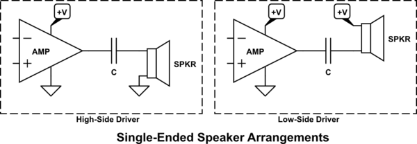
A problem with single-ended drivers is that speakers are rather complex loads that don't work nearly as well when there is a DC current bias present. If the only thing your amplifier can do is drive a voltage that is between ground and the \$+V\$ rail, then the mid-point of each swing will have a DC bias to it. (This isn't necessarily the case with the bridge-tied load. Which is an advantage.) To fix this DC component of the single-ended driver, a capacitor is inserted which will rapidly charge to a nominal voltage that is just enough so that the speaker's driven lead will oscillate above and below the voltage at the other end of the speaker. Like this:
<!-- Begin schematic: In order to preserve an editable schematic, please
don't edit this section directly.
Click the "edit" link below the image in the preview instead. -->
<!-- End schematic -->
That capacitor goes a long way. But it does need to be fairly large-valued so that it offers little impedance to the AC signals of interest. Given audio, this tends to mean close to a milli-Farad.
----------
The rail voltages required for a speaker, if you can afford a bipolar supply, is \$V=\pm\sqrt{2 P R}\$, where \$P\$ is the power you want and \$R\$ is the speaker's impedance. When the voltage supply is only a single voltage rail, you need twice that much. None of this counts for the needed overhead required to drive the circuitry. So you need to plan at least an extra volt or two, added to whatever you compute (or more.)
With \$R=8\:\Omega\$ and \$P=1\:\textrm{W}\$ this pencils out to \$V=\pm 4\:\textrm{V}\$. Or \$V=8\:\textrm{V}\$, if only a single supply rail. You also need to account for that overhead. So you can see that the voltages required for your power supply can become inconvenient if you seek significant power output into \$8\:\Omega\$ speakers. (A reason why \$4\:\Omega\$ speakers are often used then.)
The bridge-tied arrangement gets the full swing on either side, going oppositely to each other. So this allows it to appear (for these purposes) as though it has a bipolar supply when it actually doesn't. A reason why bridge-tied loads can be important when only a single, low-voltage supply rail is available.
----------
None of the above deals with something else that is very important with these single-ended speaker drivers. The capacitor helps solve the DC bias current problem, by charging itself up to just the right voltage so that the speaker can swing above and below it's reference (ground or +V.) But you need to be able to pull upward on the capacitor/speaker combo, which requires sourcing current, and you need to be able to pull downward on the capacitor/speaker combo, which requires sinking current. The driver needs to be able to do both.
Optimally, you'd have the ability to source and sink with both abilities approximately equal to each other and together sufficient for the needs of the speaker. Your arrangement has a BJT that is pretty good at sourcing current, but only \$R_7\$ to sink it. \$R_7\$ can be reduced in value to allow it to sink more current, but you pay a heavy price -- excessive power in several devices. Sometimes, that's okay. But it is almost always worth the effort to replace it.
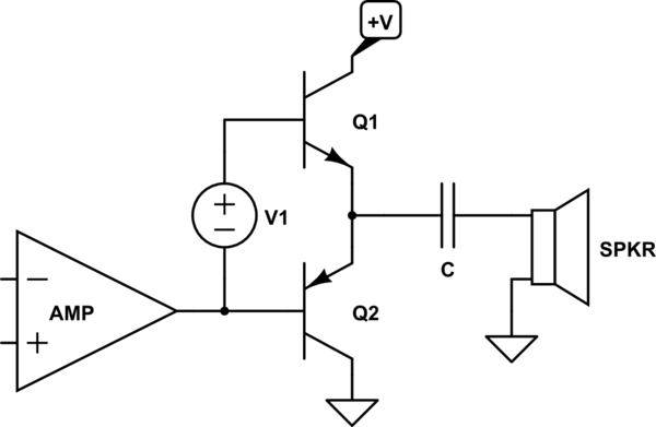
It's much better to have an active device on both sides. So you need to think about replacing \$R_7\$ with a transistor. Then you've got an active source and an active sink to drive the speaker. This is why you almost always see a speaker driver circuit that looks something like:
<!-- Begin schematic: In order to preserve an editable schematic, please
don't edit this section directly.
Click the "edit" link below the image in the preview instead. -->
<!-- End schematic -->
The voltage source shown there is designed to provide about two diode drops worth of voltage difference between the two bases of the two BJTs, so that they can both be active at the same time. Both are emitter-follower arrangements and their emitters will just follow the left-side amplifier stage's output voltage (with some relative DC bias, perhaps.) As the left-side amplifier slews its voltage up and down, so should the BJT emitters just follow that behavior.
The PNP sinks current actively and the NPN sources current actively. If you imagine pulling down on the paired base arrangement there, that will pull down on the PNP base, which will pull down *hard* on the PNP emitter sinking current actively. Likewise, if you pull up on the paired base arrangement, that will pull up on the NPN base, which will pull up *hard* on the NPN emitter, sourcing current actively. The main thing here is to make sure there is sufficient voltage between the bases that the two emitters can both be actively *on* and will therefore follow their base voltages up and/or down.
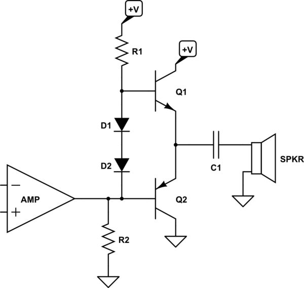
This circuit needs to have a source of base currents. This can come from the left-side amplifier, if it is capable of developing the necessary voltage and current compliances. Often, though, a very cheap "hack" is to just use the following as a starting point:
<!-- Begin schematic: In order to preserve an editable schematic, please
don't edit this section directly.
Click the "edit" link below the image in the preview instead. -->
<!-- End schematic -->
That's pretty crappy from a number of perspectives. But it does work after a fashion and with some serious limitations. You can read something about the limits here: [Effect of the Load on a Class AB Amplifier][1]. So I won't belabor it further, here.
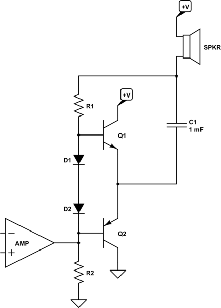
An improvement is to replace \$R_1\$ with a current source. This can be done similarly to what is done with the LM380 (see the red-boxed portion of the circuit shown here -- [Transfer function of a LM380 power amp][2]), but it is often done by bootstrapping using the output capacitor, instead. As follows:
<!-- Begin schematic: In order to preserve an editable schematic, please
don't edit this section directly.
Click the "edit" link below the image in the preview instead. -->
<!-- End schematic -->
Because \$C_1\$ develops a relatively fixed DC voltage across it during operation, and because \$V_{BE}\$ of \$Q_1\$ doesn't vary too much either (few hundred millivolts, or so), there is a relatively constant voltage across \$R_1\$. This tends to mean that there is a relatively constant current through \$R_1\$, which is an improvement on the prior topology.
----------
I've gone far enough here. There are additional improvements to the output stage I haven't even nodded at. For higher power, there each single BJT shown above might be replaced by *banks* of BJTs. Also, if you look back at the [Transfer function of a LM380 power amp][2] mentioned above, you will see that they've done something *interesting* with the low-side BJT (\$Q_2\$ in my circuits above, but \$Q_{11}\$ and \$Q_{12}\$ in theirs.)
The point is that there is a lot to be done just for designing the power supply rails and the output stage itself (which doesn't have significant gain but can sink and source significant currents.) And then you can work on the idea of a proper pre-amplifier stage for your microphone. And then finally, work on an intermediate stage (or two) with the gain you want. You can sometimes combine all this into a single added stage. (For example, look at [Cant understand an ab amplifier diagram][3].) But you really need to have some basic ideas available and the ability to work through some kind of useful analysis, if you want to try such things.
That's it for now.
[1]: https://electronics.stackexchange.com/questions/324895/effect-of-the-load-on-a-class-ab-amplifier/324935#324935
[2]: https://electronics.stackexchange.com/questions/273867/transfer-function-of-a-lm380-power-amp/273901#273901
[3]: https://electronics.stackexchange.com/questions/281753/cant-understand-an-ab-amplifier-diagram/281838#281838