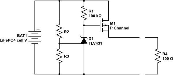
The two requirements (reverse protection & reverse polarity) are not easily met in the same single device.
By itself a MOSFET's Vgs is too poorly defined between parts and not sharp enough yto make a good low battery cutout.
By adding the world's lowest cost IC and two or three resistors you can meet both needs.
A P Channel MOSFET in the +ve lead, drain (not source) to B+, source (not drain) to Load+ and gate to B-, will provide FET which is turned on with correct battery polarity.
Now add a [**TLV431 shunt regulator**](http://www.onsemi.com/pub_link/Collateral/TLV431A-D.PDF) from FET gate to ground and ise two resistors to program it to turn om when Vbat is above a preset limit. Add a 3rd resistor gate to B+ to turn the FET off when the TLV431 is off.
I nominated a 1.25V TLV431 rather than a 2.5V TL431 as the device cathode pulls down to Vref - 0.6V at best (based on my experiences and a logical result of the internal structure) and nominally to about Vref.
With 1.25V as Vref in the TLV431 and say 3 volts Vbat that leaves (3-1.25v) = 1.75V Vgs for the MOSFET, meaning it needs Vgsth of more like 1V to work well with 1.75V on the gate. MOSFETS that meet this spec are not common but do exist.
If desired an NChannel FET can be used but the level switching circuit will probably be slightly more complex.
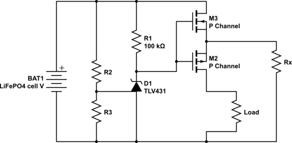
A single MOSFET will protect against reverse polarity but, as Bruce Abbot noted, does not fully protect against deep discharge due to the body diode conducting. To protect against both over-discharge and reverse polarity two back to back MOSFETs are needed
The first diagram below shows the 1 FET version with reverse polarity protection and limited low voltage protection.
For reverse polarity only omit R1, R2, R3, D1, and connect the the FET gate to groumnd. This is the standard reverse polarity protection circuit which turned up decades ago - I don't know who first thought of it but somebody attempted to parent the concept long long after it was commonplace.
Direct gate grounding is OK for Vbattery << Vgsmax.
For combined reverse polarity and low voltage cutout: When polarity is correct and battery voltage falls below set voltage the FET turns off and the body diode will be placed in series with the load - so available voltage drops from say 3V1 to maybe 2V4 (0.7V drop due to inferior diode structure). If the load was eg a white LED with Vf ~= 3.0V in normal operation then current drain would drop to a very small @ of normal.
In the second diagram the 2nd FET (both P Channel), with opposite d-s polarity to the first stops conduction via the FETS. A sbefore the R2 R3 discharge path remains and R2 should be as large as other design parameters allow.
**Fig 1 - Reverse polarity protection, low voltage adds a 0.7V+ drop diode in discharge path.**
<!-- Begin schematic: In order to preserve an editable schematic, please
don't edit this section directly.
Click the "edit" link below the image in the preview instead. -->

<!-- End schematic -->
**Fig 2 - Reverse polarity protection, low voltage disconnects load.**
Rx is notionally required to turn on back-to-back FET pair but in practice tends to be unneeded. Use Rx = 10 megohm if desired.
<!-- Begin schematic: In order to preserve an editable schematic, please
don't edit this section directly.
Click the "edit" link below the image in the preview instead. -->

<!-- End schematic -->
______________________________
Minumum discharge voltage for a LiFePO4 cell umder loads of under C are usually in the 3.0 - 3.1V range. Under heavy loads. 1C 10C - ... lower voltages are usually due to voltage dropp from internal impedance. 3.2V is extremely conservative.
The circuit above drains the battery with R2 + R3 when the FET is off. So to minimise off mode drain R2 & R3 should be as large as possible while minmising Vset due to bias currents in the resistors.
A possibly suitable part - depends on desired max current [NTJS3151P](http://www.onsemi.com/pub_link/Collateral/NTJS3151P-D.PDF) - example only.