Experimental arrangement
I was trying to design a differential amplifier in which the collector resistances of the transistors are 2.2 kΩ and are biased at 1 mA and are supplied with Vcc= +/-5 V.
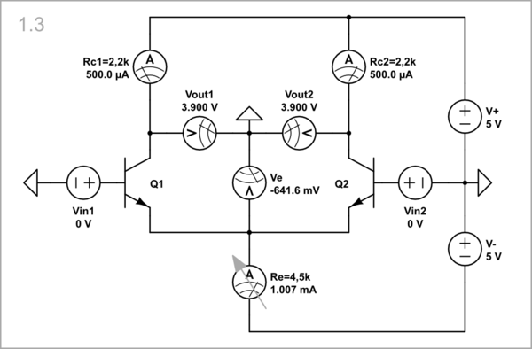
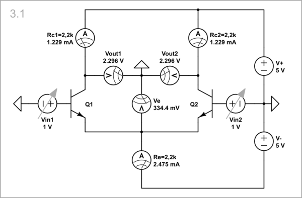
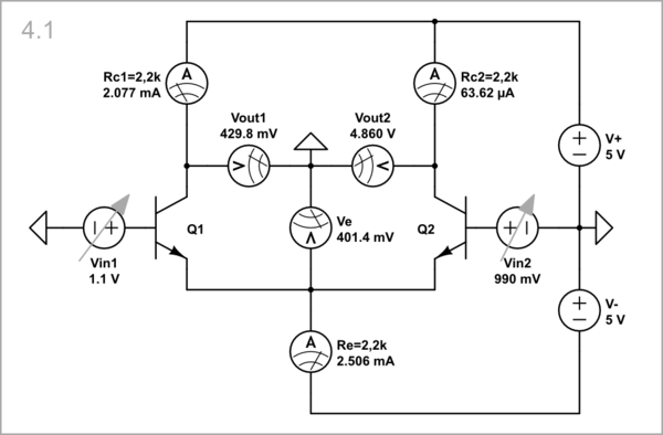
I have illustrated your arrangement (with corrected Ie = 2 mA) by a little unusual CircuitLab simulation consisting only of voltage sources and meters (see the schematics below). My idea was to visualize the most important electrical quantities without cluttering the schematic. For this purpose, I have presented the collector resistors as ammeters with an internal resistance of 2.2 kΩ, and the emitter resistor - through a voltmeter with an internal resistance of 2.2 kΩ. Simply put, think of them as "visualized resistors". The collector and emitter voltages are visualized with ordinary (perfect) voltmeters. Note that their "black probes" are connected to ground (the midpoint of the power supply).
Experiments
I suggest revealing the ideas behind this famous circuit (figuratively called "long-tailed pair" in the past) by doing a number of step-by-step experiments. The first of them (framed in black) is your circuit; the others (framed in pale gray) explore its operation modes.
Setting the operating point
Ic1 = Ic2 = 1 mA

simulate this circuit – Schematic created using CircuitLab
Ic1 = Ic2 = 1.5 mA

Ic1 = Ic2 = 0.5 mA

Differential mode
Vin1 = 10 mV, Vin2 = -10 mV

Vin1 = -10 mV, Vin2 = 10 mV

Common mode
Vin1 = Vin2 = 1 V

Vin1 = Vin2 = -1 V

Mixed mode
Vin1 = 1.1 V, Vin2 = 0.99 V

Vin1 = 0.99 V, Vin2 = 1.1 V

