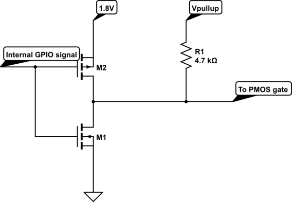
The output is very likely a [push pull][1] stage which has a (relatively) low output resistance.
What you effectively have is this (assuming you are using a CMOS device)
<!-- Begin schematic: In order to preserve an editable schematic, please
don't edit this section directly.
Click the "edit" link below the image in the preview instead. -->

<!-- End schematic -->
The output when high will have M2 on and M1 off.
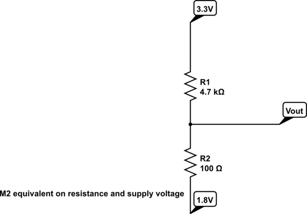
The output of this stage when high will have a typical resistance to 1.8V of perhaps a few tens (sometimes higher) of ohms; the voltage divider formed of M2 and the pullup resistor will maintain the output voltage at close to the GPIO drive voltage of 1.8V
You *could* use an [open drain][2] output but ensure it is safe to use with a 3.3V pullup (that will be in the datasheet).
The *effective* circuit in the high output state is this:
<!-- Begin schematic: In order to preserve an editable schematic, please
don't edit this section directly.
Click the "edit" link below the image in the preview instead. -->

<!-- End schematic -->
From the [voltage divider][3] principle, the voltage at Vout will be 1.83125V (assuming the on resistance of M2 is 100 ohms).
You should not normally pull a push pull / totem pole output *beyond* its supply voltages whether that be positive or negative.
[1]: https://electronics.stackexchange.com/questions/225218/push-pull-cmos-output-stage-overcoming-the-distortion-problem
[2]: https://electronics.stackexchange.com/questions/312401/is-sinking-mode-and-open-drain-the-same-concept-in-electronics
[3]: https://en.wikipedia.org/wiki/Voltage_divider