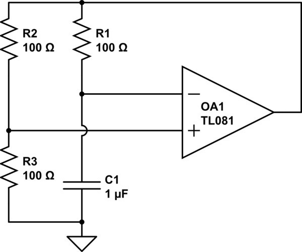
You can't have frequency linearly proportional to RC, but you can have the period so controlled. Frequency is then k/RC.
You could try a circuit based on this back of envelope sketch.
**WARNING** these component values will not make a sensible oscillator, though it may well simulate OK, they were merely the defaults when I created the schematic. You will have to figure out sensible values.
<!-- Begin schematic: In order to preserve an editable schematic, please
don't edit this section directly.
Click the "edit" link below the image in the preview instead. -->

<!-- End schematic -->
This is a relaxation oscillator. Positive feedback is achieved via R2 and R3, with timing control via R1 and C1.
Note that this circuit as drawn requires dual rails, as C1 and R3 go to ground. It is straightforwrd to modify for single rail operation with an effective ground point.
The beauty of this circuit is that even if low values of R1 are loading the output of the amplifier such that its output drops, the drop applies both to the voltage on the timing resistor R1 **and** the hysteresis chain R2/R3, so the period remains unaffected by amplifier output impedance. The same goes for variations of the voltage rails.
This behaviour is in contrast to what would happen if you used a schmidt trigger inverter, like the 74HC14 for instance, in place of the amplifier+R2+R3 combination. It has an input hysteresis that is more or less constant, regardless of rail voltage and output drop, so these would affect the frequency.. You would not get 50% duty cycle either.
It is reasonable to have R2=R3, this doesn't provide a freq = 1/RC condition, but it's not far off. You can tweak the R2/R3 ratio to get exactly that formula if you want. Do it either analytically as an exercise, or play with values in a simulator. I'd tend to just throw a couple of 10k or 100k in those positions without further thought.
You will have to make sure that the hysteresis that you choose with R2 and R3 stays within the common mode input range of the amplifier. The default amplifier that comes up in the schematic is a TL081, which includes the +ve rail but not GND in its common mode range. There are many other amplifier choices which can include ground or both rails, but they are not necessary unless you want to use extreme R2/R3 ratios.
**CAVEATS**
This circuit is linear and 50% duty cycle to first order, that is, for when the op-amp is behaving **ideally**.
Real op-amps will have a finite slew rate and gain bandwidth product. Once the delay after switching becomes a significant part of the period, the frequency will fall back from the linear law it had at lower frequencies. Use a fast enough op-amp.
Although both the hysteresis and charging current are controlled by the same pin, the hysteresis value is only relevant at the moment of switching, whereas the charging current is valid for the whole period. If the output of the op-amp varies over the period, due to excess current being drawn by R1 and R2, or by excess output loading, or by non-infinite gain, the output frequency will fall short of the linear law at higher frequencies. Keep the minimum value of R1 sufficiently high.
If the resistors become too large, offset currents taken by the amplifier will become a significant fraction of the currents passing through the resistors, and will distort the duty cycle away from 50%.
There are better designs that have fewer defects, working in current rather than voltage mode for instance, if better linearity at high freqeuncies is needed.