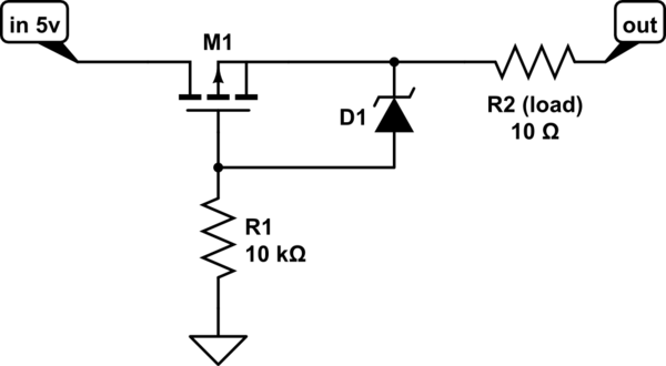
I have been looking over multiple designs for ideal diodes using FET transistors such as the circuits from these posts:
https://electronics.stackexchange.com/questions/290284/pmosfet-ideal-diode-for-24v
https://electronics.stackexchange.com/questions/223935/understanding-an-ideal-diode-made-from-a-p-channel-mosfet-and-pnp-transistors
and from this site:
http://jiggerjuice.info/electronics/projects/power/ideal-diode.html
The part that I don't understand is why they use so many other components in their designs. My question is if the following circuit I designed functions the same as the ones linked above.
<!-- Begin schematic: In order to preserve an editable schematic, please
don't edit this section directly.
Click the "edit" link below the image in the preview instead. -->

<!-- End schematic -->
The zener diode is being used to protect the gate terminal on the FET.
edit: for use as a high side half wave rectifier:
[![Ideal Diode][1]][1]
[1]: https://i.sstatic.net/pJonl.jpg