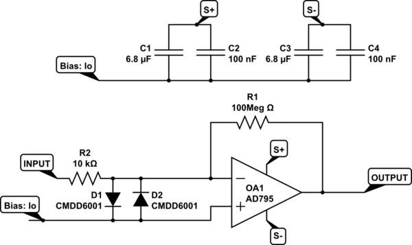
I'm trying to build a trans-impedance amplifier shown in the circuit below.
However, with my op-amp of choice, the [AD795][1], I'm a bit confused by their circuit board notes and how to implement them. The input node sends a current in pico-amp range, and the TIA converts it into a voltage at the output. Considering how tiny the input is, it's very critical to maintain the pico-amp resolution at the input. Looking at the datasheet, it shows some notes about this.
<!-- Begin schematic: In order to preserve an editable schematic, please
don't edit this section directly.
Click the "edit" link below the image in the preview instead. -->

<!-- End schematic -->
The first thing they mention is a guard ring in figure 34. Using the unconnected pin pad 1, I can connect it to the bias and draw a guard trace around the input signal path in a no-copper-pour zone so all there is is the signal trace and the guard ring. I can add vias within the ring, as evidenced by what Analog Devices did with this [evaluation board for the ADA4350][2]. AD shows the guard being tied to the same potential as the non-inverting node, and that is what I attempted to do. Is this the correct way to form a guard ring, or am I doing it completely wrong?
EDIT: Below is my latest attempt at a guard ring, along with the 3D view of it. As you can see, the exposed copper trace is tied to Io, the non-inverting input, while surrounding the inverting input node and the corresponding traces. The ring is also replicated on the bottom plane.
[![Guard V3][4]][4]
[![Guard V3 3D view][5]][5]
[1]: https://www.analog.com/media/en/technical-documentation/data-sheets/AD795.pdf
[2]: https://www.analog.com/en/design-center/evaluation-hardware-and-software/evaluation-boards-kits/EVAL-ADA4530-1.html
[3]: https://www.digikey.com/product-detail/en/keystone-electronics/11218/36-11218-ND/2170346
[4]: https://i.sstatic.net/op9b9.png
[5]: https://i.sstatic.net/eUr1s.png