Please try this.
[![enter image description here][1]][1]
1. Let R2 be 1 kilo ohms
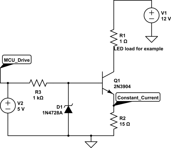
2. Place a zener of reverse voltage of say 2.7 V (for discussion sake) between base and the ground and make sure it is biased properly when MCU is driving it.
3. Change emitter resistor(R1) to 14 ohms
4. Now we have a constant 2.7 V applied across the base whenever the zener is driven (reverse voltage)
5. Assuming base drop of 0.7 V, we will have 2 V across this emitter resistor all the time.
6. It corresponds to a current of 2 V / 14 ohms which is roughly 142 mA.
7. Note that this is independent of positive voltage (10 V to 20 V)
8. Please find a darlington transistor for high ß
9. Depending of MCU voltage you can choose zener voltage and do similar math again to choose new emitter resistor value
10. No. Doesn't work with V+ floating.
11. R3 can be your load (LEDs for example)
All above points refers to reference designators in OP's question
_____________________________
Will upload the circuit soon
**Example only** Schematics:
Below is the sweep done for 12 V supply in 2 V steps until 20 V. you can run the simulation and tweak values.
<!-- Begin schematic: In order to preserve an editable schematic, please
don't edit this section directly.
Click the "edit" link below the image in the preview instead. -->
[![enter image description here][2]][2]

<!-- End schematic -->
*Below text uses references in my circuit*
Zener and R2(in my circuit) together act as negative feedback for this system and hence when current tries to increase, the emitter voltage will increase which tends to decrease the applied base emitter voltage for the transistor there by reducing the gain a little and the nice the collector current accordingly.
[1]: https://i.sstatic.net/Bs9LZ.png
[2]: https://i.sstatic.net/vICT1.png