6
\$\begingroup\$

I am trying to create a circuit which will allow me to scale and offset a voltage (be it AC or DC) to within the range of the Arduino ADC.

The voltage could be anything between + and - 250V, but I also need to have good sensitivity over lower voltage ranges too.

To this end I am looking at a circuit whereby you can vary the voltage range that it expects the input to be and amplify/attenuate it accordingly. How I will be making the decision and setting the different gains is for another topic for now. I am only interested in the scaling and offsetting at the moment.

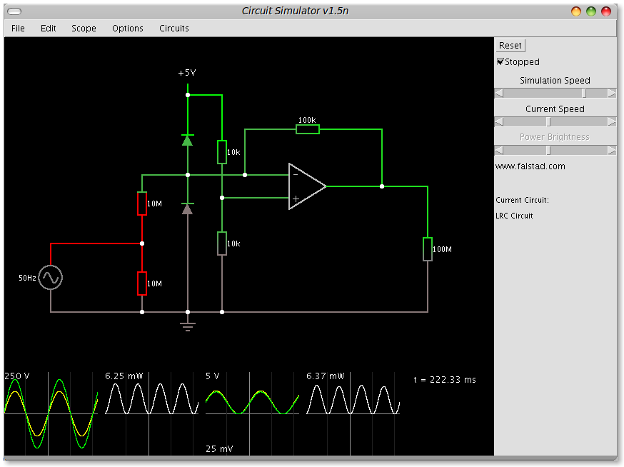
So far I have come up with this circuit:
enter image description here

Which appears to do just what I want for the +/- 250V range. I don't know how "safe" this circuit is, and if I am endangering any of the components with the 250V or not. The graphs at the bottom are (left to right) the input voltage, the power consumption of the bottom 10M resistor, the voltage across the 100M resistor (which is simulating the Arduino ADC input) and the power consumption of the upper 10M resistor.

Now, if I drop the input voltage to just +/- 2.5V and tweak the op-amp feedback resistor accordingly, for some reason the offset voltage the op-amp is adding jumps right up. I don't know for sure if this is the fault of the simulator I am using, or if it is really what will happen, as I haven't yet breadboarded this circuit (I guess that's the next stage).

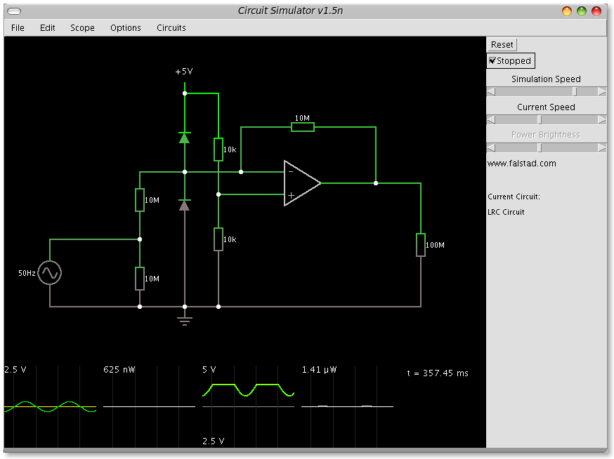
This is the output from the 2.5V version:
enter image description here

You can see how the offset has jumped up and the output is clipping massively.

If I drop the lower 10K resistor to the virtual ground offset voltage divider to just 3.3K it compensates, but that's not nice - I would like to just vary the one resistor.

The op-amp is (will be) a 5V single supply rail-to-rail I/O one.

The two diodes are to protect the input of the op-amp against over voltage - I don't know if this circuit strictly needs them, but I guess it doesn't hurt to have them there.

Also, I don't know if the resistor values are quite what I want - I chose them to keep the power consumption right down and the impedance right up. I don't want them to impact the frequency response of the circuit more than I can help - the input waveform could be anything from DC up to around 500KHz or so, and I need that reproducing at the ADC end as faithfully as I can. (I know the Arduino can only really sample at lower speeds than that, but the Arduino is just for experimenting - the final system will use a dsPIC with 1.1Msps ADC).

So, what can I do to A) get a more stable offset, B) allow the varying of the input sensitivity without nuking either the op-amp or the ADC, and C) make the circuit safe to connect to, for example, a European mains voltage?

\$\endgroup\$

2 Answers 2

6
\$\begingroup\$

Several comments:

  1. Add component designators to your schematic. It is difficult to talk about the circuit otherwise.

  2. You appear to be a little confused about resistor dividers. You have two resistor on the input, but only one is doing anything. The resistor to ground is just a load on the input but otherwise has no bearing on your circuit. It sortof looks like the two input resistors (component designators would definitely help) are meant to be a divider that didn't get hooked up right.

  3. Yes, you can use opamps for gains below 1, but you might as well use resistor dividers instead. Also keep in mind that at best opamps are specified as stable for unity gain magnitude, but not below. You would have to add your own compensation for that.

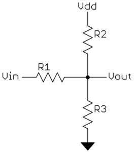
  4. Three resistors, one from the input voltage, one to ground, and one to the supply can be adjusted such that the input voltage range maps reasonably well to the 0-5V A/D range without any active parts. You can then use the opamp as a voltage buffer because the output of the resistor divider may not have low enough impedance.

  5. Instead of changing gains, I would just have a few different gain setups driving different A/D pins. As long as the voltages are properly clipped, they won't hurt being out of range. The full 220V signal may be out of range for the high sensitivity A/D input, so you ignore that and only use the low sensitivity reading. When the signal level is low, the high sensitivity input won't be clipped, so you can use that. Nothing needs to change except in the firmware, which decides which input to use for the particular magnitude of input signal.

  6. 500 kHz is a lot for the high value resistors you show. Those should work at 50 Hz, but at 1000 times higher frequency the parasitic capacitance will be significant compared to those resistances.

Added:

If whatever software you are using doesn't allow for component designators, use something that does. At least use that when drawing the schematic for other people to see. Simulators are overrated anyway. They have their uses, but all too often they seem to make the user forget he has a brain of his own. For a trivial circuit like yours, it would take longer to enter it into a simulator than to simply think it out.

You can do a lot with a three-resistor divider as I mentioned above:

This can't always exactly fill the 0-Vdd output range with the input signal. But even when it can't, there is usually a good enough solution. Generally the more you need to attenuate, the easier it is to get the output into the desired range.

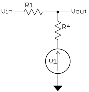
To analyze this circuit, note that by themselves R2 and R3 form a voltage divider of Vdd. This can be thought of as a voltage between Vdd and ground with a specific impedance (see Thevanin):

Where R4 = R2 // R3. How you can see we have a simple two-resistor voltage divider. The divider gain is R4/(R1+R4) and the output impedance is R1//R4. From 7th grade math we know that whatever this circuit does to the input voltage can be described by:

Vout = Vin(M) + B

You can find M and B easily enough from the above equation from any two different points. In your case, Vdd = 5V, so you want the output to be symmetric around half that, or 2.5V. So at Vin=0 you want Vout=2.5. Two other obvious known points are the peaks of the input waveform. Let's pick the negative one, so at Vin=-250 Vout=0. Now M and B can be easily solved.

If you want to find a exact solution, you can write the equations for M and B in terms of R1, R4, and V1. As long as V1 is more than 0 and less than Vdd, a exact solution is possible. From the simplified second schematic, it should be obvious that:

M = R4/(R1 + R4)
B = V1 * R1 / (R1 + R4)

Note that this system is underconstrained as there are 3 unknowns and only 2 equations. The extra degree of freedom can be expressed as the final output impedance of Vout, which is R1//R4.

You have enough here to write all the equations and solve them. That's no longer electronics but grade school arithmetic, so that's your job. Instead I'll take a less exact but more intuitive hack at it here.

Let's say you want the output impedance to not exceed 10 kΩ. We know the attenuation will be high, so R1 will be significantly larger than R4. For simplicity, let's simply make R4 = 10 kΩ. That will make the output impedance a little less than 10 kΩ. You have a 500V input range and want a 5V output range, so the divider gain should be 1/100. Again to make things simple, we'll just make R1 = 100*R4 = 1MΩ. That actually results in a gain of 1/101, but a little margin is a good idea and you'd have to get 1% resistors as it is to guarantee the gain isn't more than 1/100. So far we have:

R1 = 1 MΩ
R4 = 10 kΩ

At this high attenuation ratio, B pretty much equals V1, so let's just make V1 = 2.5V. Now we still need to get R2 and R3 from R4. From the values above, each should be 20 kΩ. However, we're making some approximations and it's good to allow for a little slop anyway, so I'd start with the next lower common value of 18 kΩ.

Now you need to plug all that in and compute the output voltage at the peaks of the input voltage, taking into account inaccuracies in the resistors. I'll leave that as a exercise to you, but the values above are either good enough or pretty close for a starting point.

\$\endgroup\$
2
  • \$\begingroup\$ 1: I would love to but the sim software doesn't let you. 2: what should I do here then to get it right? 4: Any chance of a schematic for this? 5: That's a great idea - it would mean a bigger PIC though in the final design, which isn't a problem. 6: Can I use lower resistors and keep the current down somehow so I don't have to use one the size of an apartment block when using 220V? \$\endgroup\$
    – Majenko
    Commented Nov 26, 2011 at 0:43
  • \$\begingroup\$ That's some fantastic info there Olin, thanks. I'm off to tinker with resistor dividers now. \$\endgroup\$
    – Majenko
    Commented Nov 26, 2011 at 16:49
3
\$\begingroup\$

The offset voltage is increasing as you have increased the gain and you have the non inverting input set above "mid point".

With the top circuit there is actually attenuation, so the opamp doesn't have to drive it's output very hard to keep the inverting input at 2.5V.

When you increase Rf to 10Meg, the output has to drive it's output to the necessary voltage to match the input current and keep the inverting input at 2.5V.
For example, with 0V on the input, then the output must swing to 5V to keep the inverting input at 2.5V. Basically if you have Rin the same as Rf, and you know the input voltage (0V) the midpoint voltage at -IN (2.5V) then it's easy to work out what the top of the voltage divider (opamp OUT) should be (5V)
If your signal is swinging around a different point (0v) than the opamp midpoint (2.5V) then when you change the gain you will also alter the effect the DC offset (e.g. 2.5V) has.

EDIT - If you are happy to use as many opamps as necessary, then the easiest way would be to have a fixed input voltage divider followed by a non inverting unity gain buffer and then a few opamps with different gains. You can also use a few "taps" on the input voltage divider then use e.g. a couple of OptoMOS to route the signal appropriately (these are useful for AC/DC setting to bypass the capacitor too)
As Olin mentions any parasitic capacitance will create a low pass filter which may have quite a low cutoff, so you have to be aware of this when designing for your highest frequencies a couple of pF will make a big difference with 10 Megaohms (I would stick to <= 1 Megaohm) The input impedance will also need to be very high (>100 Megaohm) to prevent attenuation so a FET input opamp would be best.
As far as dual rails go they can make life easier here if you need DC coupling, a charge pump can be used (the rails don't need to be symmetrical) followed by some filtering, or of course a switching regulator. You have the signal swinging round 0V up to the (opamp before the) ADC then level shift.

I would look at a a few input stages for oscilloscopes, as this seems to have much the same requirements. There are plenty out there, check some of the service manuals for commercial scopes out, and also stuff like Bitscope and DSO Nano/Quad.

Probably wouldn't hurt to pick up a good book on opamps too if you haven't got one - a decent freely available one is Opamps for Everyone.
IIRC it goes into great detail on the simultaneous equations involved in calculating the straight line equation constants (as Olin goes into a little with the resistor divider) so if you want to keep a single supply Olin's advice combined with the first couple of chapters would be good reading.
Personally I would go with the dual rail as it makes things like maintaining a constant DC -> AC input impedance easier and prevents issues with midpoint bias when you switch from 1x to 10x probe setting, effectively altering R1 in Olin's example.

The goal of 500kHz should make things a bit easier as you don't have to worry as much about high speed problems. You may want to have a filter rolling off a fair bit before 500kHz though for anti-aliasing purposes - I'd say around 350kHz to keep filtering reasonably easy. I assume you'll want quite a few division settings, (down to say 100mV/div) and also you want to divide the screen into 10. I'll also assume you will be using a probe with a 10x setting.
So on the maximum division setting: 500/10x probe = 50V, divided by 1:10 input voltage divider = 5V. For a typical scope input impedance of 1 Megaohm, this would equate to 900k and 100k for the divider.
For the lowest range of 100mV/div, you would need a gain of 50 from input to ADC. 1V input divided by 10 = 100mV, times 50 equals 5V.
Splitting the gain over a couple of opamps will make the other gain settings easier, and maintain a decent bandwidth (higher gain = lower opamp bandwidth)
Say one opamp with e.g. selectable gains of (something like) 1, 2 and 5 feeding another with gains of 1, 2 and 10 (using standard CMOS multiplexers like 74HC4051/2) gives you a few options from 1 to 50. Then a final level shifting ADC buffer opamp, and you can do it all with a quad (FET input) opamp package.

\$\endgroup\$
6
  • \$\begingroup\$ Can you maybe suggest a way to change the circuit, or a better circuit, that would keep the offset the same? I am happy to incorporate as many op-amps as needed, and to separate gain/attenuation from offset if needed. I don't have a negative rail at the moment, but one could be provided if required. \$\endgroup\$
    – Majenko
    Commented Nov 25, 2011 at 19:59
  • \$\begingroup\$ @Majenko - I edited the answer a bit. I found scope schematics very useful for examples of solutions to this type of problem. \$\endgroup\$
    – Oli Glaser
    Commented Nov 26, 2011 at 0:36
  • \$\begingroup\$ Funny you should say that - a scope is what I am making ;) \$\endgroup\$
    – Majenko
    Commented Nov 26, 2011 at 1:11
  • \$\begingroup\$ Aha! :-) Depending on what you want to achieve (bandwidth, range, mechanical or software controls, etc) and at what cost, the analogue front end can be quite a challenge, but well worth it IMHO (had a go myself a couple of times with moderate success) Then there's the rest of it to design of course :-) Good luck. \$\endgroup\$
    – Oli Glaser
    Commented Nov 26, 2011 at 4:00
  • \$\begingroup\$ Software control, <=500KHz, +/-250V. The software side of it is not a problem, nor the digital aspects - just the analogue front end... \$\endgroup\$
    – Majenko
    Commented Nov 26, 2011 at 16:41

Your Answer

By clicking “Post Your Answer”, you agree to our terms of service and acknowledge you have read our privacy policy.

Not the answer you're looking for? Browse other questions tagged or ask your own question.