added 287 characters in body
Source Link
nidhin
  • 8.4k
  • 3
  • 31
  • 47

Consider the circuit diagram of a center-tapped full wave rectifier where D1 is forward biased and D2 is reverse biased.enter image description here
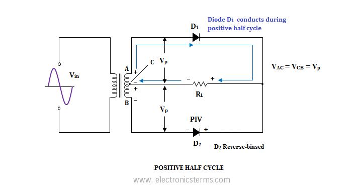
The maximum reverse voltage appearing across will be 2*Vp. Where Vp is the amplitude of input signal.

But VpSo the diode that is used in a center-tapped full wave rectifier should have a PIV of atleast twice the peak voltage of input sine wave. Otherwise diode breakdown will happen and current will flow through the reverse biased diode. And the circuit is not a rectifier anymore.

Similarly, PIV for a full wave bridge rectifier will be Vp.

Consider the circuit diagram of a center-tapped full wave rectifier where D1 is forward biased and D2 is reverse biased.enter image description here

The maximum reverse voltage appearing across will be 2*Vp. Where Vp is the amplitude of input signal.

But Vp for a full wave bridge rectifier will be Vp.

Consider the circuit diagram of a center-tapped full wave rectifier where D1 is forward biased and D2 is reverse biased.enter image description here

The maximum reverse voltage appearing across will be 2*Vp. Where Vp is the amplitude of input signal.

So the diode that is used in a center-tapped full wave rectifier should have a PIV of atleast twice the peak voltage of input sine wave. Otherwise diode breakdown will happen and current will flow through the reverse biased diode. And the circuit is not a rectifier anymore.

Similarly, PIV for a full wave bridge rectifier will be Vp.

Source Link
nidhin
  • 8.4k
  • 3
  • 31
  • 47

Consider the circuit diagram of a center-tapped full wave rectifier where D1 is forward biased and D2 is reverse biased.enter image description here

The maximum reverse voltage appearing across will be 2*Vp. Where Vp is the amplitude of input signal.

But Vp for a full wave bridge rectifier will be Vp.