added 322 characters in body
Source Link
Asy
  • 115
  • 4

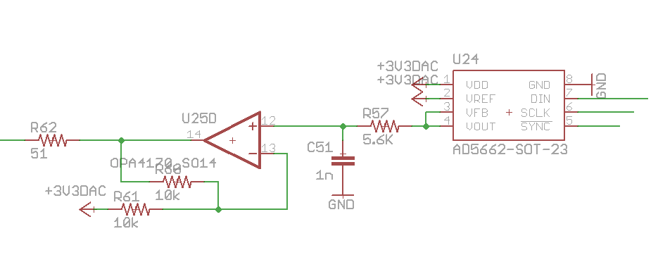
I'm working on modifying a board, while going through its schematic design I came across a section where a DAC output into the range of [0, +3.3V], which is then supposedly gained to +/-3.3V range, see extract below:
circuit

U24 is the an AD5662 DAC, with both VDD and Vref at +3.3V.

U25D is an OPA4170 opamp, with supply at +/-3.3V. It's in a non-inverting configuration. The transfer function is derived from:

$$V_{+}=\frac{1}{2}(V_{out}-3.3)$$, so $$V_{out}=2V_{+}+3.3$$

Two things that don't make sense to me:

  1. Input range of 0 to +3.3V would be amplified to [+3.3v, 9.9V] according to this transfer function, since the positive supply is only at +3.3V,that would result in Vout to be constantly at the rail.

  2. Since the input voltage is always positive, how can the output of the opamp ever be negative?

I would think that this is probably a mistake and that the left side of R61 should be connected to -3.3V, resulting in a transfer function $$V_{out}=2V_{+}-3.3$$, which would work as advertised.

However, the production board does indeed follow the schematic, and the opamp converts a strictly positive Vout (sinusoid with offset) from the DAC to a zero-centered signal. This wouldn't surprise me if the DAC output is capacitively coupled to the opamp. But R57 and C51 act as a low-pass filter, so I'm kinda stumped here.

Clearly this board's design works as advertised, but it doesn't make sense to me why. Can anyone point out where I'm making mistakes in my analysis?


Edit: Seems like I made a pretty silly mistake in my transfer function derivation, should be $$V_{+}=\frac{1}{2}(V_{out}-3.3)+3.3$$ to account for the voltage divider potential as being offset from 3.3 rather than ground.

Thanks all the for the help, I wish I could mark everyone's as solution.

I'm working on modifying a board, while going through its schematic design I came across a section where a DAC output into the range of [0, +3.3V], which is then supposedly gained to +/-3.3V range, see extract below:

circuit

U24 is the an AD5662 DAC, with both VDD and Vref at +3.3V.

U25D is an OPA4170 opamp, with supply at +/-3.3V. It's in a non-inverting configuration. The transfer function is derived from:

$$V_{+}=\frac{1}{2}(V_{out}-3.3)$$, so $$V_{out}=2V_{+}+3.3$$

Two things that don't make sense to me:

  1. Input range of 0 to +3.3V would be amplified to [+3.3v, 9.9V] according to this transfer function, since the positive supply is only at +3.3V,that would result in Vout to be constantly at the rail.

  2. Since the input voltage is always positive, how can the output of the opamp ever be negative?

I would think that this is probably a mistake and that the left side of R61 should be connected to -3.3V, resulting in a transfer function $$V_{out}=2V_{+}-3.3$$, which would work as advertised.

However, the production board does indeed follow the schematic, and the opamp converts a strictly positive Vout (sinusoid with offset) from the DAC to a zero-centered signal. This wouldn't surprise me if the DAC output is capacitively coupled to the opamp. But R57 and C51 act as a low-pass filter, so I'm kinda stumped here.

Clearly this board's design works as advertised, but it doesn't make sense to me why. Can anyone point out where I'm making mistakes in my analysis?


Edit: Seems like I made a pretty silly mistake in my transfer function derivation, should be $$V_{+}=\frac{1}{2}(V_{out}-3.3)+3.3$$ to account for the voltage divider potential as being offset from 3.3 rather than ground.

Thanks all the for the help, I wish I could mark everyone's as solution.

Source Link
Asy
  • 115
  • 4

Amplify 0 to 3.3V input to +/-3.3V

I'm working on modifying a board, while going through its schematic design I came across a section where a DAC output into the range of [0, +3.3V], which is then supposedly gained to +/-3.3V range, see extract below:

circuit

U24 is the an AD5662 DAC, with both VDD and Vref at +3.3V.

U25D is an OPA4170 opamp, with supply at +/-3.3V. It's in a non-inverting configuration. The transfer function is derived from:

$$V_{+}=\frac{1}{2}(V_{out}-3.3)$$, so $$V_{out}=2V_{+}+3.3$$

Two things that don't make sense to me:

  1. Input range of 0 to +3.3V would be amplified to [+3.3v, 9.9V] according to this transfer function, since the positive supply is only at +3.3V,that would result in Vout to be constantly at the rail.

  2. Since the input voltage is always positive, how can the output of the opamp ever be negative?

I would think that this is probably a mistake and that the left side of R61 should be connected to -3.3V, resulting in a transfer function $$V_{out}=2V_{+}-3.3$$, which would work as advertised.

However, the production board does indeed follow the schematic, and the opamp converts a strictly positive Vout (sinusoid with offset) from the DAC to a zero-centered signal. This wouldn't surprise me if the DAC output is capacitively coupled to the opamp. But R57 and C51 act as a low-pass filter, so I'm kinda stumped here.

Clearly this board's design works as advertised, but it doesn't make sense to me why. Can anyone point out where I'm making mistakes in my analysis?