added 439 characters in body
Source Link
jbord39
  • 4.4k
  • 1
  • 19
  • 25

A flip flop is two opposite phase latches back to back.

A latch consists (in this case) of a back to back inverter. To write into a latch you must overcome the feedback inverter (trying to write old value) with the input inverter which is driving the initial bitnode. One solution to this problem is to cut off the feedback inverter whenever the latch is transparent.

This is the purpose of the switches S2/S4: they prevent the second inverter in each chain from writing back to the input, while the latches are open.

This prevents contention, speeds up the latch, and reduces power consumption. Very common in VLSI. It also removes the need to size the input inverter stronger than the feedback inverter.

Opposite phase is the key word which helps you decide on what type of switch to use.

For a positive edge flip flop, the second latch must OPEN when the clock goes high.

Consider the situations:

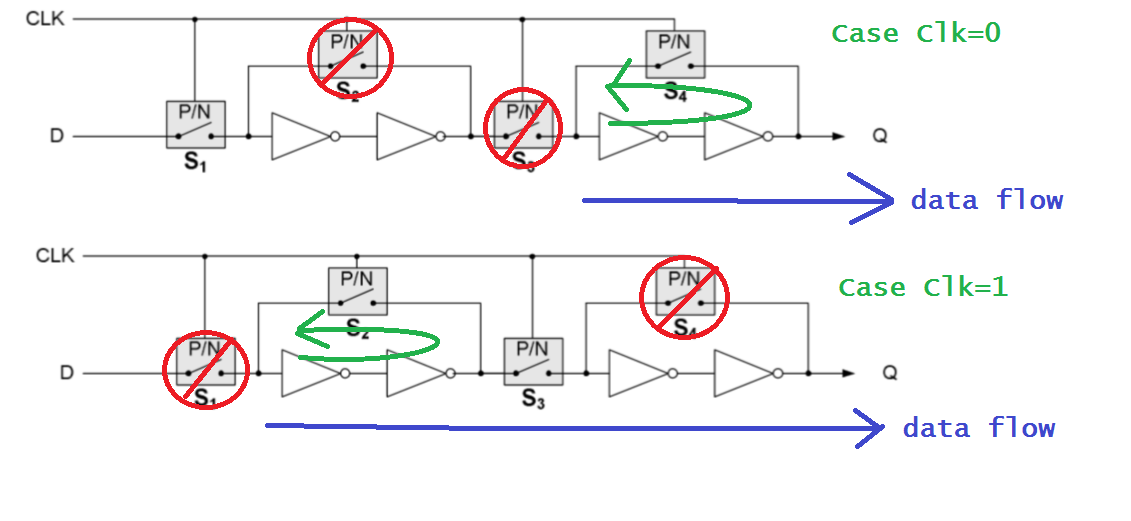
CLK high: master latch closed, slave latch opened => S1=off,S2=on,S3=on,S4=off


CLK low : master latch open, slave latch closed => S1=on,S2=off,S3=off,S4=on

From here it easy to see that:

S1 = PMOS
S2 = NMOS
S3 = NMOS
S4 = PMOS

Although typically the switches S1/S3 would be transmission gates. And S2/S4 would be tri-state inverters built into the feedback inverters of each latch.

EDIT

basic dff

Added a picture. Green circle arrow shows feedback. Red means switch is off. Blue shows where the output data comes from.

So, when clock is low the data is stored in the master latch.
When clock goes high, the master latch is cut off from D. Simultaneously the data from the master latch passes through the slave latch. So, rising-edge FF.

A flip flop is two opposite phase latches back to back.

A latch consists (in this case) of a back to back inverter. To write into a latch you must overcome the feedback inverter (trying to write old value) with the input inverter which is driving the initial bitnode. One solution to this problem is to cut off the feedback inverter whenever the latch is transparent.

This is the purpose of the switches S2/S4: they prevent the second inverter in each chain from writing back to the input, while the latches are open.

This prevents contention, speeds up the latch, and reduces power consumption. Very common in VLSI. It also removes the need to size the input inverter stronger than the feedback inverter.

Opposite phase is the key word which helps you decide on what type of switch to use.

For a positive edge flip flop, the second latch must OPEN when the clock goes high.

Consider the situations:

CLK high: master latch closed, slave latch opened => S1=off,S2=on,S3=on,S4=off


CLK low : master latch open, slave latch closed => S1=on,S2=off,S3=off,S4=on

From here it easy to see that:

S1 = PMOS
S2 = NMOS
S3 = NMOS
S4 = PMOS

Although typically the switches S1/S3 would be transmission gates. And S2/S4 would be tri-state inverters built into the feedback inverters of each latch.

EDIT

basic dff

Added a picture. Green circle arrow shows feedback. Red means switch is off. Blue shows where the output data comes from.

So, when clock is low the data is stored in the master latch.
When clock goes high, the master latch is cut off from D. Simultaneously the data from the master latch passes through the slave latch. So, rising-edge FF.

added 157 characters in body
Source Link
jbord39
  • 4.4k
  • 1
  • 19
  • 25

A flip flop is two opposite phase latches back to back.

A latch consists (in this case) of a back to back inverter. To write into a latch you must overcome the feedback inverter (trying to write old value) with the input inverter which is driving the initial bitnode. One solution to this problem is to cut off the feedback inverter whenever the latch is transparent.

This is the purpose of the switches S2/S4: they prevent the second inverter in each chain from writing back to the input, while the latches are open.

This prevents contention, speeds up the latch, and reduces power consumption. Very common in VLSI. It also removes the need to size the input inverter stronger than the feedback inverter.

Opposite phase is the key word which helps you decide on what type of switch to use.

For a positive edge flip flop, the second latch must OPEN when the clock goes high.

Consider the situations:

CLK high: master latch closed, slave latch opened => S1=off,S2=on,S3=on,S4=off


CLK low : master latch open, slave latch closed => S1=on,S2=off,S3=off,S4=on

From here it easy to see that:

S1 = PMOS
S2 = NMOS
S3 = NMOS
S4 = PMOS

Although typically the switches S1/S3 would be transmission gates. And S2/S4 would be tri-state inverters built into the feedback inverters of each latch.

A flip flop is two opposite phase latches back to back.

A latch consists (in this case) of a back to back inverter. To write into a latch you must overcome the feedback inverter (trying to write old value) with the input inverter which is driving the initial bitnode. One solution to this problem is to cut off the feedback inverter whenever the latch is transparent.

This is the purpose of the switches S2/S4: they prevent the second inverter in each chain from writing back to the input, while the latches are open.

This prevents contention, speeds up the latch, and reduces power consumption. Very common in VLSI. It also removes the need to size the input inverter stronger than the feedback inverter.

Opposite phase is the key word which helps you decide on what type of switch to use.

For a positive edge flip flop, the second latch must OPEN when the clock goes high.

Consider the situations:

CLK high: master latch closed, slave latch opened => S1=off,S2=on,S3=on,S4=off


CLK low : master latch open, slave latch closed => S1=on,S2=off,S3=off,S4=on

From here it easy to see that:

S1 = PMOS
S2 = NMOS
S3 = NMOS
S4 = PMOS

Although typically the switches S1/S3 would be transmission gates. And S2/S4 would be tri-state inverters built into the feedback inverters of each latch.

added 472 characters in body
Source Link
jbord39
  • 4.4k
  • 1
  • 19
  • 25

A flip flop is two opposite phase latches back to back.

A latch consists (in this case) of a back to back inverter. To write into a latch you must overcome the feedback inverter (trying to write old value) with the input inverter which is driving the initial bitnode. One solution to this problem is to cut off the feedback inverter whenever the latch is transparent.

This is the purpose of the switches S2/S4: they prevent the second inverter in each chain from writing back to the input, while the latches are open.

This prevents contention, speeds up the latch, and reduces power consumption. Very common in VLSI. It also removes the need to size the input inverter stronger than the feedback inverter.

Opposite phase is the key word which helps you decide on what type of switch to use.

For a positive edge flip flop, the second latch must OPEN when the clock goes high.

Consider the situations:

CLK high: master latch closed, slave latch opened => S1=off,S2=on,S3=on,S4=off


CLK low : master latch open, slave latch closed => S1=on,S2=off,S3=off,S4=on

From here it easy to see that:

S1 = PMOS
S2 = NMOS
S3 = NMOS
S4 = PMOS

A flip flop is two opposite phase latches back to back.

A latch consists (in this case) of a back to back inverter. To write into a latch you must overcome the feedback inverter (trying to write old value) with the input inverter which is driving the initial bitnode. One solution to this problem is to cut off the feedback inverter whenever the latch is transparent.

This is the purpose of the switches S2/S4: they prevent the second inverter in each chain from writing back to the input, while the latches are open.

This prevents contention, speeds up the latch, and reduces power consumption. Very common in VLSI. It also removes the need to size the input inverter stronger than the feedback inverter.

Opposite phase is the key word which helps you decide on what type of switch to use.

For a positive edge flip flop, the second latch must OPEN when the clock goes high.

Consider the situations:

CLK high: master latch closed, slave latch opened => S1=off,S2=on,S3=on,S4=off


CLK low : master latch open, slave latch closed => S1=on,S2=off,S3=off,S4=on

From here it easy to see that:

S1 = PMOS
S2 = NMOS
S3 = NMOS
S4 = PMOS
Source Link
jbord39
  • 4.4k
  • 1
  • 19
  • 25
Loading