added 115 characters in body
Source Link
D.A.S.
  • 148k
  • 3
  • 56
  • 190

In my first job in 1975 at Bristol Aerospace (now Magellan) we had a good aviation and NASA qualified draftsmen, but one kept making D and E size drawings so microfiche would not create false dots from optical blurring, so I had to convince him to use A, B, and C size maximum by condensing symbol gaps and reducing font size. Because I often had to work with 20 pages at a time.

In my next job, our draftsman was an illustrator who could convert any messy high-density drawing on a paper napkin into a beautiful readable work of art in hours, not days (like the block diagram of each chip on a motherboard). He ended up at my fourth job too and was the best draftsman we had, just like what one would see from Tektronix, HP and Hitachi.

Yes, they used symbol templates.

In the mid 1970s when we designed a system with about 40 PCAs we had no simulation tools and no quickturn PCB shops and no decent layout tools. So we drew it on a 4x scale grid Mylar with coloured pencils for G code track width and sent it to Toronto for optical digitizations. The checkplots were sent back in a week for approval and then boards in two weeks.

That was 1976. Fast-forward 15 years later; I made photo tools at a lithographic printshop from the design EEs the same day and two-sided boards ready the next day. For six-layer Getek and FPC boards, I got three quotes in one hour only using a table of numbers without Gerber files and had prototype boards (10) delivered in 48 hours to one week depending on urgency $xK.

I did the same thing for half-etched dotted-line tinned brass shields for 1 GHz radio shields for prototypes and had them made locally in two days using delivered two-sided phototools. Then the panel had breakaway tabs inside edge and could be assembled and soldered to board in minutes using high power soldering tools or micro-propane torch for walls with a removable folded lid (circa mid 1990s).

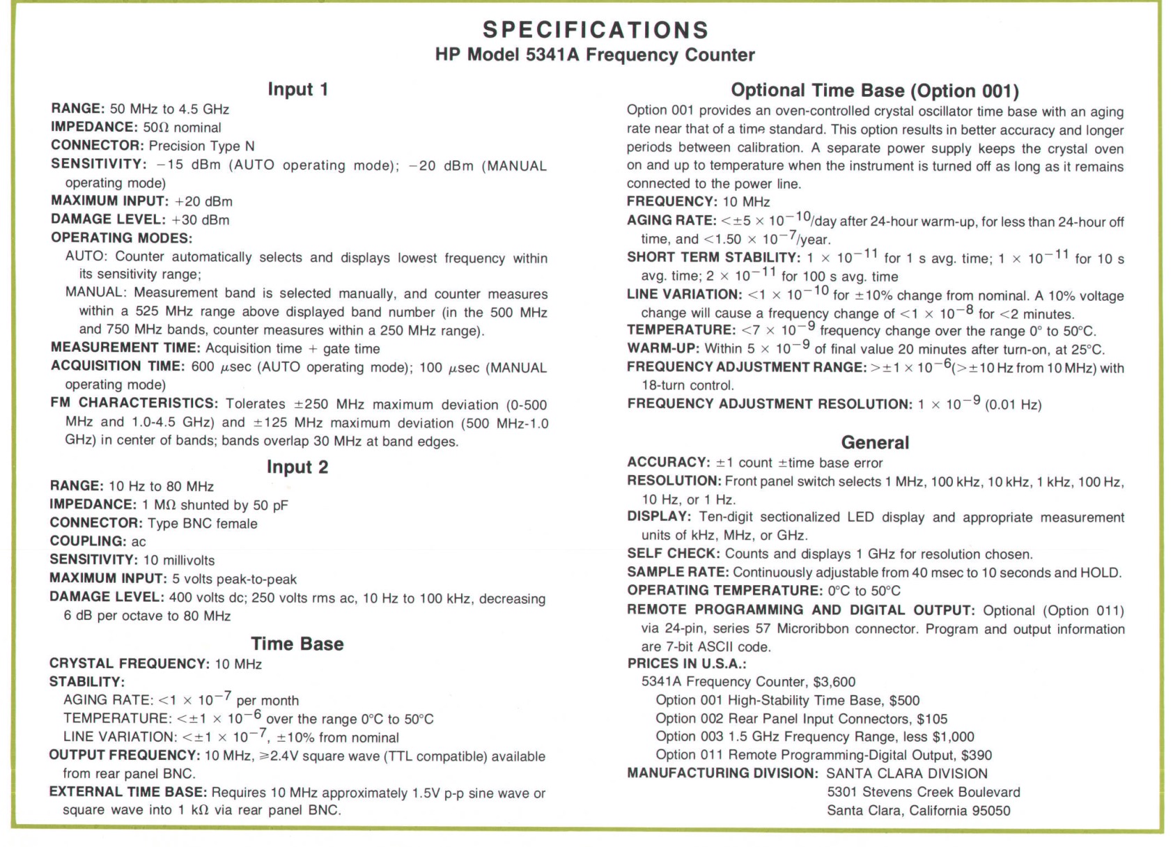
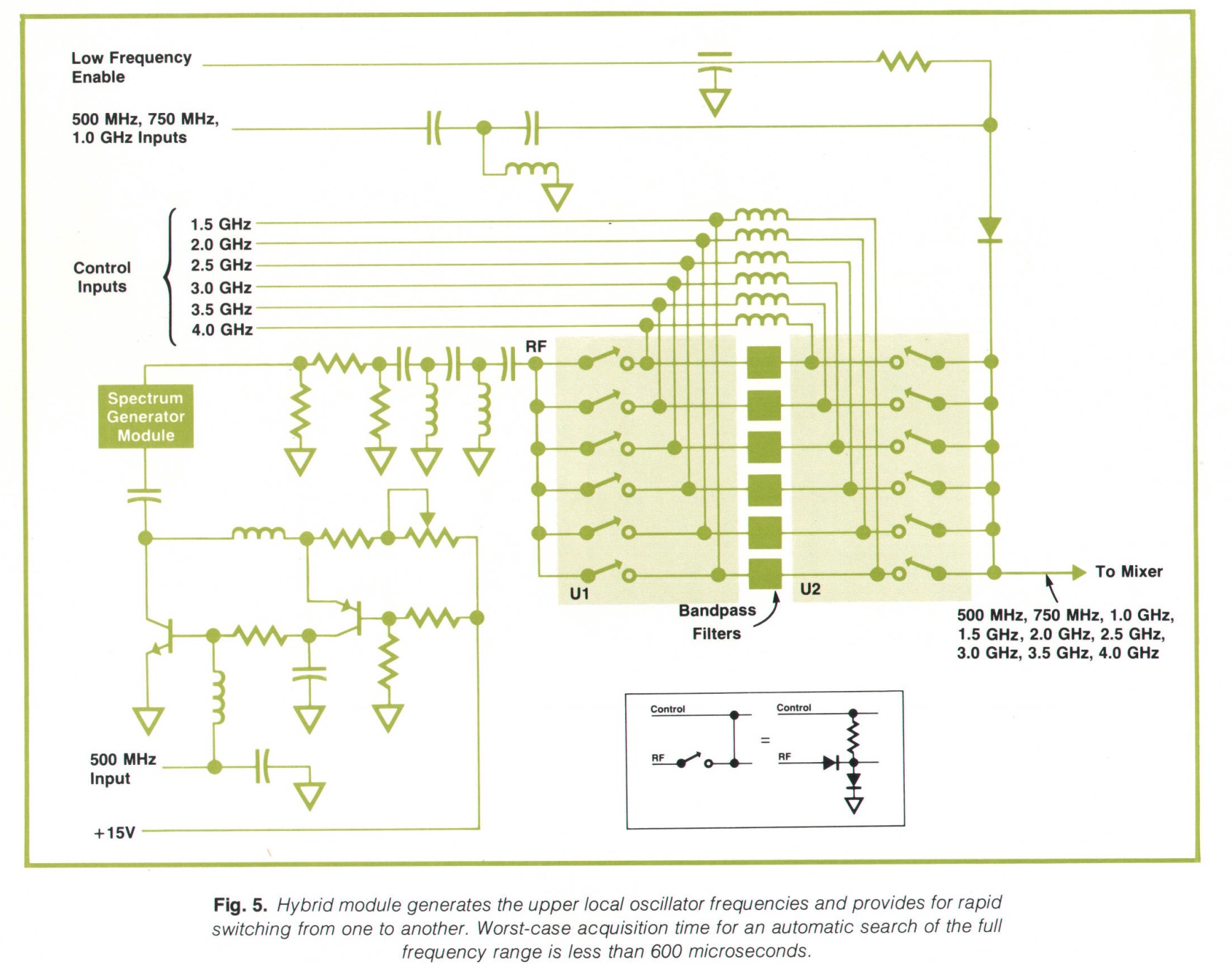
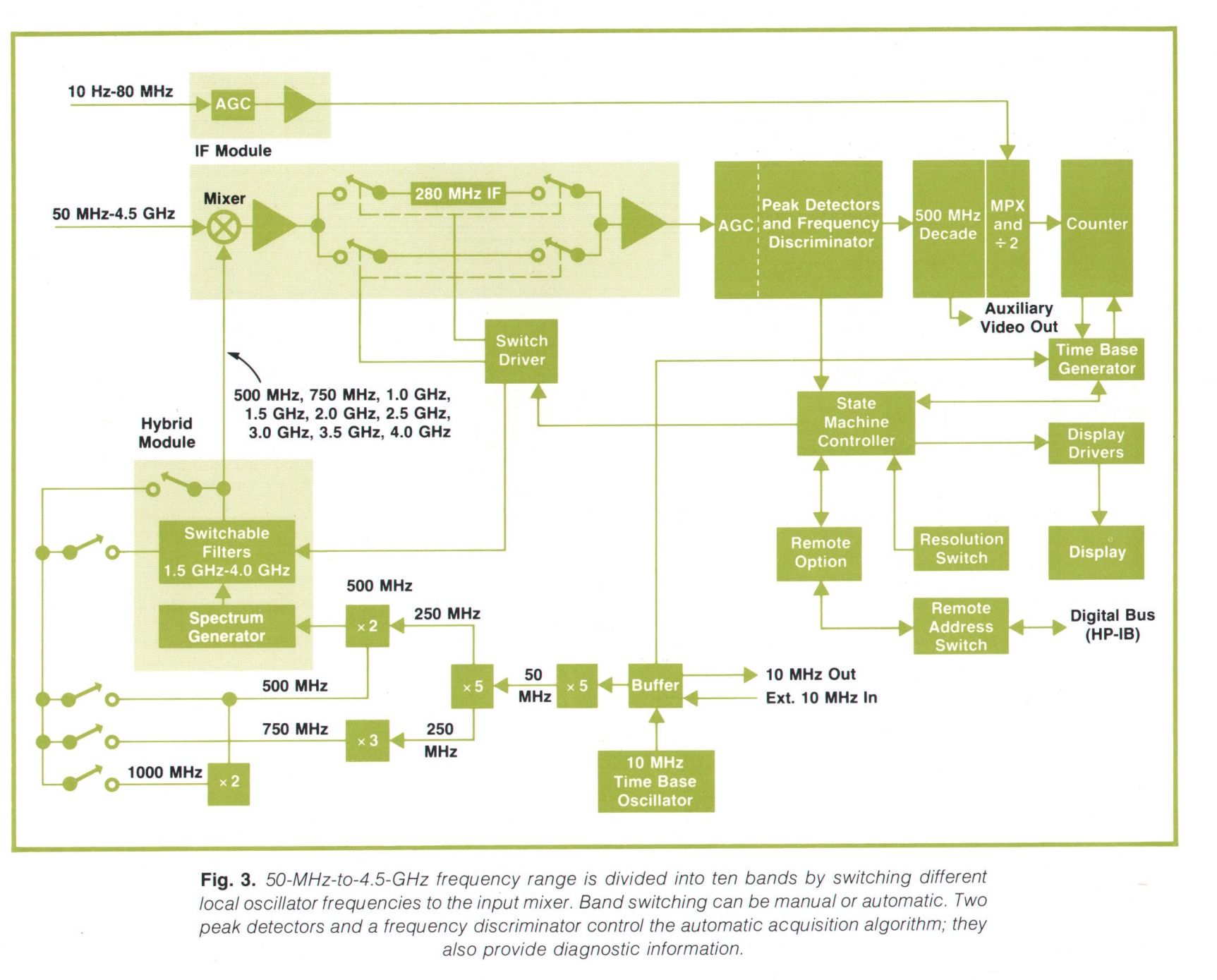
Here's a 4.5 GHz counter simplified schema & block diagram from the HP journal for an instrument we bought in 1976 with 1 Hz resolution:

Enter image description here

Enter image description here

When I ask OPs or users for specifications, I expect they will learn to have details like this and share the relevant ones. But often they are oblivious to the need for good specifications to make a good design.

Enter image description here

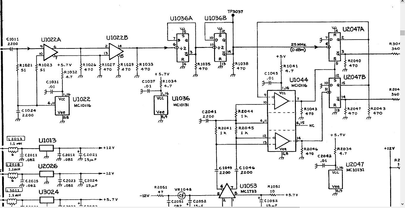
Fast Forward to 1985 with this TEKTRONIX SA492 Spectrum Analyzer. This may only be 1% of the whole schematic and was done in an easy to understand and the manual was in a hierarchical manner like PADS dwg's were done.

enter image description here

This is one the best models for electronic schematics to follow and designers who choose REFDES for ease of locating from board to schematic. Earth ground symbol is important here because of the shielding design unlike triangle symbols which often ignore noise. Later I'll post the 32MB manual link from my dropbox. Experienced Current Mode Logic (ECL) designers will recognize the sub nano second latency and rise time logic here. LDO users should note the necessary RLC filters on the input for RF applications.

In my first job in 1975 at Bristol Aerospace (now Magellan) we had a good aviation and NASA qualified draftsmen, but one kept making D and E size drawings so microfiche would not create false dots from optical blurring, so I had to convince him to use A, B, and C size maximum by condensing symbol gaps and reducing font size. Because I often had to work with 20 pages at a time.

In my next job, our draftsman was an illustrator who could convert any messy high-density drawing on a paper napkin into a beautiful readable work of art in hours, not days (like the block diagram of each chip on a motherboard). He ended up at my fourth job too and was the best draftsman we had, just like what one would see from Tektronix, HP and Hitachi.

Yes, they used symbol templates.

In the mid 1970s when we designed a system with about 40 PCAs we had no simulation tools and no quickturn PCB shops and no decent layout tools. So we drew it on a 4x scale grid Mylar with coloured pencils for G code track width and sent it to Toronto for optical digitizations. The checkplots were sent back in a week for approval and then boards in two weeks.

That was 1976. Fast-forward 15 years later; I made photo tools at a lithographic printshop from the design EEs the same day and two-sided boards ready the next day. For six-layer Getek and FPC boards, I got three quotes in one hour only using a table of numbers without Gerber files and had prototype boards (10) delivered in 48 hours to one week depending on urgency $xK.

I did the same thing for half-etched dotted-line tinned brass shields for 1 GHz radio shields for prototypes and had them made locally in two days using delivered two-sided phototools. Then the panel had breakaway tabs inside edge and could be assembled and soldered to board in minutes using high power soldering tools or micro-propane torch for walls with a removable folded lid (circa mid 1990s).

Here's a 4.5 GHz counter simplified schema & block diagram from the HP journal for an instrument we bought in 1976 with 1 Hz resolution:

Enter image description here

Enter image description here

When I ask OPs or users for specifications, I expect they will learn to have details like this and share the relevant ones. But often they are oblivious to the need for good specifications to make a good design.

Enter image description here

Fast Forward to 1985 with this TEKTRONIX SA492 Spectrum Analyzer. This may only be 1% of the whole schematic and was done in an easy to understand and the manual was in a hierarchical manner like PADS dwg's were done.

enter image description here

This is one the best models for electronic schematics to follow and designers who choose REFDES for ease of locating from board to schematic. Earth ground symbol is important here because of the shielding design unlike triangle symbols which often ignore noise. Later I'll post the 32MB manual link from my dropbox.

In my first job in 1975 at Bristol Aerospace (now Magellan) we had a good aviation and NASA qualified draftsmen, but one kept making D and E size drawings so microfiche would not create false dots from optical blurring, so I had to convince him to use A, B, and C size maximum by condensing symbol gaps and reducing font size. Because I often had to work with 20 pages at a time.

In my next job, our draftsman was an illustrator who could convert any messy high-density drawing on a paper napkin into a beautiful readable work of art in hours, not days (like the block diagram of each chip on a motherboard). He ended up at my fourth job too and was the best draftsman we had, just like what one would see from Tektronix, HP and Hitachi.

Yes, they used symbol templates.

In the mid 1970s when we designed a system with about 40 PCAs we had no simulation tools and no quickturn PCB shops and no decent layout tools. So we drew it on a 4x scale grid Mylar with coloured pencils for G code track width and sent it to Toronto for optical digitizations. The checkplots were sent back in a week for approval and then boards in two weeks.

That was 1976. Fast-forward 15 years later; I made photo tools at a lithographic printshop from the design EEs the same day and two-sided boards ready the next day. For six-layer Getek and FPC boards, I got three quotes in one hour only using a table of numbers without Gerber files and had prototype boards (10) delivered in 48 hours to one week depending on urgency $xK.

I did the same thing for half-etched dotted-line tinned brass shields for 1 GHz radio shields for prototypes and had them made locally in two days using delivered two-sided phototools. Then the panel had breakaway tabs inside edge and could be assembled and soldered to board in minutes using high power soldering tools or micro-propane torch for walls with a removable folded lid (circa mid 1990s).

Here's a 4.5 GHz counter simplified schema & block diagram from the HP journal for an instrument we bought in 1976 with 1 Hz resolution:

Enter image description here

Enter image description here

When I ask OPs or users for specifications, I expect they will learn to have details like this and share the relevant ones. But often they are oblivious to the need for good specifications to make a good design.

Enter image description here

Fast Forward to 1985 with this TEKTRONIX SA492 Spectrum Analyzer. This may only be 1% of the whole schematic and was done in an easy to understand and the manual was in a hierarchical manner like PADS dwg's were done.

enter image description here

This is one the best models for electronic schematics to follow and designers who choose REFDES for ease of locating from board to schematic. Earth ground symbol is important here because of the shielding design unlike triangle symbols which often ignore noise. Later I'll post the 32MB manual link from my dropbox. Experienced Current Mode Logic (ECL) designers will recognize the sub nano second latency and rise time logic here. LDO users should note the necessary RLC filters on the input for RF applications.
added 341 characters in body
Source Link
D.A.S.
  • 148k
  • 3
  • 56
  • 190

In my first job in 1975 at Bristol Aerospace (now Magellan) we had a good aviation and NASA qualified draftsmen, but one kept making D and E size drawings so microfiche would not create false dots from optical blurring, so I had to convince him to use A, B, and C size maximum by condensing symbol gaps and reducing font size. Because I often had to work with 20 pages at a time.

In my next job, our draftsman was an illustrator who could convert any messy high-density drawing on a paper napkin into a beautiful readable work of art in hours, not days (like the block diagram of each chip on a motherboard). He ended up at my fourth job too and was the best draftsman we had, just like what one would see from Tektronix, HP and Hitachi.

Yes, they used symbol templates.

In the mid 1970s when we designed a system with about 40 PCAs we had no simulation tools and no quickturn PCB shops and no decent layout tools. So we drew it on a 4x scale grid Mylar with coloured pencils for G code track width and sent it to Toronto for optical digitizations. The checkplots were sent back in a week for approval and then boards in two weeks.

That was 1976. Fast-forward 15 years later; I made photo tools at a lithographic printshop from the design EEs the same day and two-sided boards ready the next day. For six-layer Getek and FPC boards, I got three quotes in one hour only using a table of numbers without Gerber files and had prototype boards (10) delivered in 48 hours to one week depending on urgency $xK.

I did the same thing for half-etched dotted-line tinned brass shields for 1 GHz radio shields for prototypes and had them made locally in two days using delivered two-sided phototools. Then the panel had breakaway tabs inside edge and could be assembled and soldered to board in minutes using high power soldering tools or micro-propane torch for walls with a removable folded lid (circa mid 1990s).

Here's a 4.5 GHz counter simplified schema & block diagram from the HP journal for an instrument we bought in 1976 with 1 Hz resolution:

Enter image description here

Enter image description here

When I ask OPs or users for specifications, I expect they will learn to have details like this and share the relevant ones. But often they are oblivious to the need for good specifications to make a good design.

Enter image description here

Fast Forward to 1985 with this TEKTRONIX SA492 Spectrum Analyzer. This may only be 1% of the whole schematic and was done in an easy to understand and the manual was in a hierarchical manner like PADS dwg's were done.

enter image description here

This is one the best models for electronic schematics to follow and designers who choose REFDES for ease of locating from board to schematic. Earth ground symbol is important here because of the shielding design unlike triangle symbols which often ignore noise. Later I'll post the 32MB manual link from my dropbox.

In my first job in 1975 at Bristol Aerospace (now Magellan) we had a good aviation and NASA qualified draftsmen, but one kept making D and E size drawings so microfiche would not create false dots from optical blurring, so I had to convince him to use A, B, and C size maximum by condensing symbol gaps and reducing font size. Because I often had to work with 20 pages at a time.

In my next job, our draftsman was an illustrator who could convert any messy high-density drawing on a paper napkin into a beautiful readable work of art in hours, not days (like the block diagram of each chip on a motherboard). He ended up at my fourth job too and was the best draftsman we had, just like what one would see from Tektronix, HP and Hitachi.

Yes, they used symbol templates.

In the mid 1970s when we designed a system with about 40 PCAs we had no simulation tools and no quickturn PCB shops and no decent layout tools. So we drew it on a 4x scale grid Mylar with coloured pencils for G code track width and sent it to Toronto for optical digitizations. The checkplots were sent back in a week for approval and then boards in two weeks.

That was 1976. Fast-forward 15 years later; I made photo tools at a lithographic printshop from the design EEs the same day and two-sided boards ready the next day. For six-layer Getek and FPC boards, I got three quotes in one hour only using a table of numbers without Gerber files and had prototype boards (10) delivered in 48 hours to one week depending on urgency $xK.

I did the same thing for half-etched dotted-line tinned brass shields for 1 GHz radio shields for prototypes and had them made locally in two days using delivered two-sided phototools. Then the panel had breakaway tabs inside edge and could be assembled and soldered to board in minutes using high power soldering tools or micro-propane torch for walls with a removable folded lid (circa mid 1990s).

Here's a 4.5 GHz counter simplified schema & block diagram from the HP journal for an instrument we bought in 1976 with 1 Hz resolution:

Enter image description here

Enter image description here

When I ask OPs or users for specifications, I expect they will learn to have details like this and share the relevant ones. But often they are oblivious to the need for good specifications to make a good design.

Enter image description here

Fast Forward to 1985 with this TEKTRONIX SA492 Spectrum Analyzer. This may only be 1% of the whole schematic and was done in an easy to understand and the manual was in a hierarchical manner like PADS dwg's were done.

enter image description here

This is one the best models for electronic schematics to follow and designers who choose REFDES for ease of locating from board to schematic. Earth ground symbol is important here because of the shielding design unlike triangle symbols which often ignore noise. Later I'll post the 32MB manual link from my dropbox.

In my 1stfirst job in 1975 at Bristol Aerospace (now Magellan) we had a good aviation and NASA qualified draftsmen  , but one kept making D and E size drawings so microfiche would not create false dots from optical blurring, so I had to convince him to use A, B, and C size maxmaximum by condensing symbol gaps and reducing font size. Because I often had to work with 20 pages at a time.

In my next job, our draftsman was an illustrator who could convert any messy high density dwg.on-density drawing on a paper napkin intointo a beautiful readable work of art in hours, not days. (Likelike the block diagram of each chip on a MOBOmotherboard). He ended up at my 4thfourth job too and was the best draftsman we had, just like what one would see from TekTektronix, HP and Hitachi.

Yes, they used symbol templates.

In the mid 70's1970s when we designed a system with about 40 PCA'sPCAs we had no simulation tools and no quickturn PCB shops and no decent layout tools. So we drew it on a 4x scale grid Mylar with coloured pencils for G code track width and the sent it to Toronto for Opticaloptical digitizations and. The checkplots were sent back in a week for approval and then boards in 2two weeks.

That was 1976. Fast-Forwardforward 15 years later,later; I made photo tools at a Lithographiclithographic printshop from the design EE'sEEs the same day and 2 sidedtwo-sided boards ready the next day. For 6 layerFor six-layer Getek and FPC boards, I got 3three quotes in 1one hour only using a table of numbers without GerbersGerber files and had prototype boards (10) delivered in 48 hrshours to 1one week depending on urgency $xK.

I did the same thing for half etched-etched dotted line-line tinned brass shields for 1GHz1 GHz radio shields for prototypes and had them made locally in 2two days using delivered 2 sidedtwo-sided phototools,. Then the panel had breakaway tabs inside edge and could be assembled and soldered to board in minutes using high power soldering tools or micro-propane torch for walls with a removable folded Lid.lid (circa mid 90's1990s).

Here's a 4.5GHz5 GHz counter simplified schémaschema & block diagram from the HP journal for an instrument we bought in 1976 with 1Hz1 Hz resolution. :

enter image description hereEnter image description here   

enter image description hereEnter image description here

When I ask OPs or users for specsspecifications, I expect they will learn to have details like this and share the relevant ones. But often they are oblivious to the need for good specsspecifications to make a good design.   

enter image description hereEnter image description here

In my 1st job in 1975 at Bristol Aerospace (now Magellan) we had a good aviation and NASA qualified draftsmen  , but one kept making D and E size drawings so microfiche would not create false dots from optical blurring, so I had to convince him to use A B and C size max by condensing symbol gaps and reducing font size. Because I often had to work with 20 pages at a time.

In my next job, our draftsman was an illustrator who could convert any messy high density dwg.on a paper napkin into a beautiful readable work of art in hours, not days. (Like the block diagram of each chip on a MOBO) He ended up at my 4th job too and was the best draftsman we had, just like what one would see from Tek, HP and Hitachi.

Yes they used symbol templates.

In the mid 70's when we designed a system with about 40 PCA's we had no simulation tools and no quickturn PCB shops and no decent layout tools. So we drew it on 4x scale grid Mylar with coloured pencils for G code track width and the sent to Toronto for Optical digitizations and checkplots sent back in a week for approval then boards in 2 weeks.

That was 1976. Fast-Forward 15 years later, I made photo tools at a Lithographic printshop from the design EE's same day and 2 sided boards ready next day. For 6 layer Getek and FPC boards, I got 3 quotes in 1 hour only using a table of numbers without Gerbers and had prototype boards (10) delivered in 48 hrs to 1 week depending on urgency $xK.

I did the same thing for half etched dotted line tinned brass shields for 1GHz radio shields for prototypes and had them made locally in 2 days using delivered 2 sided phototools, Then the panel had breakaway tabs inside edge and could be assembled and soldered to board in minutes using high power soldering tools or micro-propane torch for walls with a removable folded Lid. (circa mid 90's)

Here's a 4.5GHz counter simplified schéma & block diagram from the HP journal for an instrument we bought in 1976 with 1Hz resolution. enter image description here  enter image description here

When I ask OPs or users for specs, I expect they will learn to have details like this and share the relevant ones. But often they are oblivious to the need for good specs to make a good design.  enter image description here

In my first job in 1975 at Bristol Aerospace (now Magellan) we had a good aviation and NASA qualified draftsmen, but one kept making D and E size drawings so microfiche would not create false dots from optical blurring, so I had to convince him to use A, B, and C size maximum by condensing symbol gaps and reducing font size. Because I often had to work with 20 pages at a time.

In my next job, our draftsman was an illustrator who could convert any messy high-density drawing on a paper napkin into a beautiful readable work of art in hours, not days (like the block diagram of each chip on a motherboard). He ended up at my fourth job too and was the best draftsman we had, just like what one would see from Tektronix, HP and Hitachi.

Yes, they used symbol templates.

In the mid 1970s when we designed a system with about 40 PCAs we had no simulation tools and no quickturn PCB shops and no decent layout tools. So we drew it on a 4x scale grid Mylar with coloured pencils for G code track width and sent it to Toronto for optical digitizations. The checkplots were sent back in a week for approval and then boards in two weeks.

That was 1976. Fast-forward 15 years later; I made photo tools at a lithographic printshop from the design EEs the same day and two-sided boards ready the next day. For six-layer Getek and FPC boards, I got three quotes in one hour only using a table of numbers without Gerber files and had prototype boards (10) delivered in 48 hours to one week depending on urgency $xK.

I did the same thing for half-etched dotted-line tinned brass shields for 1 GHz radio shields for prototypes and had them made locally in two days using delivered two-sided phototools. Then the panel had breakaway tabs inside edge and could be assembled and soldered to board in minutes using high power soldering tools or micro-propane torch for walls with a removable folded lid (circa mid 1990s).

Here's a 4.5 GHz counter simplified schema & block diagram from the HP journal for an instrument we bought in 1976 with 1 Hz resolution:

Enter image description here 

Enter image description here

When I ask OPs or users for specifications, I expect they will learn to have details like this and share the relevant ones. But often they are oblivious to the need for good specifications to make a good design. 

Enter image description here

added 595 characters in body
Source Link
D.A.S.
  • 148k
  • 3
  • 56
  • 190
Loading
Source Link
D.A.S.
  • 148k
  • 3
  • 56
  • 190
Loading