fixed engish
Source Link
b degnan
  • 3.3k
  • 3
  • 19
  • 38

The region below threshold has generally just been a footnote; however, subthreshold operation has several desirable characteristics, such as simple physics, high-transconductance, and “sharp-edge” transitions in digital applications. In contrast, the temperature dependence of diffusion movement due to the thermal voltage terms is substantially greater than with super-threshold designs that operate through drift movement. In analog applications, subthreshold gives you high gain, and in digital applications, it can give you lower power.

A good reference for this that is not paywalled is Jen Hasler's Neuromorphic Roadmap.

Subthreshold has the highest gategain for an operational region; however, it generally breaks the classical concepts of what people are comfortable dealdealing with. You can easily see this if you start with the math, and to unify operation, use the EKV model:

$$I_{nFET}=I_{f,r} =\frac{W}{L}2 U_{T}^2\frac{\mu C_{ox}}{ \kappa}\ln^2 \left[1 + e^{\left({\kappa\left(V_g-V_{T0}\right) - V_{s,d}}\right)/\left({2 U_{T}}\right)} \right]$$

The mathematical form of \$ln^2 \left(1 + e^{\frac{x}{2}}\right)\$ between the regions of operation let's you take a Taylor Expansion around the point of operation. For your pFET, the equation is

$$I_{pFET} =I_{f,r} =\frac{W}{L}2 U_{T}^2\frac{\mu_p C_{ox}}{\kappa}\ln^2 \left[1+ e^{\left[{\left(\kappa \left(V_b -V_g+V_{thp}\right)\right)- \left(V_{b}-V_{s,d}\right)}\right]/\left({2 U_{T}}\right)} \right]$$

In the analog sense, you are looking for a high \$g_m\$, and subthreshold gives you this. In your schematic, your diff-pair is basically a source follower, and you want to have the biased transistor in subthreshold for the maximum gain on the diff-pair. In above threshold, you'd basically have no gain and a terrible amplifier. Also, the power is lower because the flux is conserved through the circuit so your current mirrors will not use more current than is supplied to them, and that current is limited by your bias transistor.

Subthreshold is not bad to design with if you understand devicesdevice physics. I have found that most issues regarding analog in subthreshold can be addressed with symmetry and careful design.

In the digital sense, the digital designer is driven by the incentive of “faster” designs. The megahertz race of the nineties and naughtiesnaughts, and the constant need for speed driven by the desire for faster software, has resulted in designers rewarding complexity over simplicity. Transistor scaling has done an excellent job of giving similar, but not perfectly scaled, transistor changes with feature size. Regarding scaling, one often hears references to “Moore’s Law”, but the concept of scaling is generally not understood by those who casually throw around the term. This has manifested in "faster" CPUs that generally can do less per Watt.

powerwall

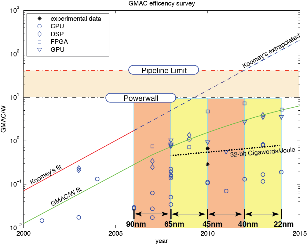
As the graph shows, the data suggests that scaling is steadily decreasing computational efficiency of digital processors. The larger question is whether this decreasing computational efficiency will trend toward an efficiency barrier asymptotically, or just have a decreased slope when compared to previous generations. There is basically a powerwall that exists if you use above threshold operation for digital devices. You can easily see this in I-V curves from a commercially available 14nm process:

enter image description here

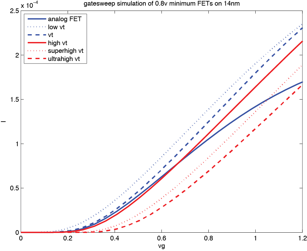
The graph above show a linear plot, and you can see that the devices are not compliant to the "square law" due to higher order effects. However, the subthreshold regime is pretty nice:

enter image description here

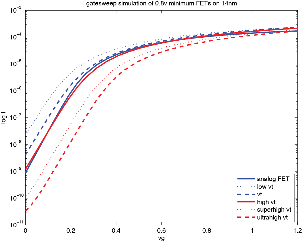
The reason that you could consider subthreshold "slow" is that the current is lower and it takes longer to charge a gate capacitor of a fixed size; however, you have fewer higher order effects.

For the best power processing per-Watt, you can just design to run in subthreshold at near threshold. If you want to "double your speed" in standard designs, you basically have to double the power. I just take my digital designs and run them in asynchronous wrappers so that I can operate them at "near threshold" where the gain is still good and I don't lose a lot of power to the higher-order issues, such as "band-to-band" tunneling that we see a lot of on 24nm and smaller nodes.

The region below threshold has generally just been a footnote; however, subthreshold operation has several desirable characteristics, such as simple physics, high-transconductance, and “sharp-edge” transitions in digital applications. In contrast, the temperature dependence of diffusion movement due to the thermal voltage terms is substantially greater than with super-threshold designs that operate through drift movement. In analog applications, subthreshold gives you high gain, and in digital applications, it can give you lower power.

A good reference for this that is not paywalled is Jen Hasler's Neuromorphic Roadmap.

Subthreshold has the highest gate for an operational region; however, it generally breaks the classical concepts of what people are comfortable deal with. You can easily see this if you start with the math, and to unify operation, use the EKV model:

$$I_{nFET}=I_{f,r} =\frac{W}{L}2 U_{T}^2\frac{\mu C_{ox}}{ \kappa}\ln^2 \left[1 + e^{\left({\kappa\left(V_g-V_{T0}\right) - V_{s,d}}\right)/\left({2 U_{T}}\right)} \right]$$

The mathematical form of \$ln^2 \left(1 + e^{\frac{x}{2}}\right)\$ between the regions of operation let's you take a Taylor Expansion around the point of operation. For your pFET, the equation is

$$I_{pFET} =I_{f,r} =\frac{W}{L}2 U_{T}^2\frac{\mu_p C_{ox}}{\kappa}\ln^2 \left[1+ e^{\left[{\left(\kappa \left(V_b -V_g+V_{thp}\right)\right)- \left(V_{b}-V_{s,d}\right)}\right]/\left({2 U_{T}}\right)} \right]$$

In the analog sense, you are looking for a high \$g_m\$, and subthreshold gives you this. In your schematic, your diff-pair is basically a source follower, and you want to have the biased transistor in subthreshold for the maximum gain on the diff-pair. In above threshold, you'd basically have no gain and a terrible amplifier. Also, the power is lower because the flux is conserved through the circuit so your current mirrors will not use more current than is supplied to them, and that current is limited by your bias transistor.

Subthreshold is not bad to design with if you understand devices. I have found that most issues regarding analog in subthreshold can be addressed with symmetry and careful design.

In the digital sense, the digital designer is driven by the incentive of “faster” designs. The megahertz race of the nineties and naughties, and the constant need for speed driven by the desire for faster software, has resulted in designers rewarding complexity over simplicity. Transistor scaling has done an excellent job of giving similar, but not perfectly scaled, transistor changes with feature size. Regarding scaling, one often hears references to “Moore’s Law”, but the concept of scaling is generally not understood by those who casually throw around the term. This has manifested in "faster" CPUs that generally can do less per Watt.

powerwall

As the graph shows, the data suggests that scaling is steadily decreasing computational efficiency of digital processors. The larger question is whether this decreasing computational efficiency will trend toward an efficiency barrier asymptotically, or just have a decreased slope when compared to previous generations. There is basically a powerwall that exists if you use above threshold operation for digital devices. You can easily see this in I-V curves from a commercially available 14nm process:

enter image description here

The graph above show a linear plot, and you can see that the devices are not compliant to the "square law" due to higher order effects. However, the subthreshold regime is pretty nice:

enter image description here

The reason that you could consider subthreshold "slow" is that the current is lower and it takes longer to charge a gate capacitor of a fixed size; however, you have fewer higher order effects.

For the best power processing per-Watt, you can just design to run in subthreshold at near threshold. If you want to "double your speed" in standard designs, you basically have to double the power. I just take my digital designs and run them in asynchronous wrappers so that I can operate them at "near threshold" where the gain is still good and I don't lose a lot of power to the higher-order issues, such as "band-to-band" tunneling that we see a lot of on 24nm and smaller nodes.
The region below threshold has generally just been a footnote; however, subthreshold operation has several desirable characteristics, such as simple physics, high-transconductance, and “sharp-edge” transitions in digital applications. In contrast, the temperature dependence of diffusion movement due to the thermal voltage terms is substantially greater than with super-threshold designs that operate through drift movement. In analog applications, subthreshold gives you high gain, and in digital applications, it can give you lower power.

A good reference for this that is not paywalled is Jen Hasler's Neuromorphic Roadmap.

Subthreshold has the highest gain for an operational region; however, it generally breaks the classical concepts of what people are comfortable dealing with. You can easily see this if you start with the math, and to unify operation, use the EKV model:

$$I_{nFET}=I_{f,r} =\frac{W}{L}2 U_{T}^2\frac{\mu C_{ox}}{ \kappa}\ln^2 \left[1 + e^{\left({\kappa\left(V_g-V_{T0}\right) - V_{s,d}}\right)/\left({2 U_{T}}\right)} \right]$$

The mathematical form of \$ln^2 \left(1 + e^{\frac{x}{2}}\right)\$ between the regions of operation let's you take a Taylor Expansion around the point of operation. For your pFET, the equation is

$$I_{pFET} =I_{f,r} =\frac{W}{L}2 U_{T}^2\frac{\mu_p C_{ox}}{\kappa}\ln^2 \left[1+ e^{\left[{\left(\kappa \left(V_b -V_g+V_{thp}\right)\right)- \left(V_{b}-V_{s,d}\right)}\right]/\left({2 U_{T}}\right)} \right]$$

In the analog sense, you are looking for a high \$g_m\$, and subthreshold gives you this. In your schematic, your diff-pair is basically a source follower, and you want to have the biased transistor in subthreshold for the maximum gain on the diff-pair. In above threshold, you'd basically have no gain and a terrible amplifier. Also, the power is lower because the flux is conserved through the circuit so your current mirrors will not use more current than is supplied to them, and that current is limited by your bias transistor.

Subthreshold is not bad to design with if you understand device physics. I have found that most issues regarding analog in subthreshold can be addressed with symmetry and careful design.

In the digital sense, the digital designer is driven by the incentive of “faster” designs. The megahertz race of the nineties and naughts, and the constant need for speed driven by the desire for faster software, has resulted in designers rewarding complexity over simplicity. Transistor scaling has done an excellent job of giving similar, but not perfectly scaled, transistor changes with feature size. Regarding scaling, one often hears references to “Moore’s Law”, but the concept of scaling is generally not understood by those who casually throw around the term. This has manifested in "faster" CPUs that generally can do less per Watt.

powerwall

As the graph shows, the data suggests that scaling is steadily decreasing computational efficiency of digital processors. The larger question is whether this decreasing computational efficiency will trend toward an efficiency barrier asymptotically, or just have a decreased slope when compared to previous generations. There is basically a powerwall that exists if you use above threshold operation for digital devices. You can easily see this in I-V curves from a commercially available 14nm process:

enter image description here

The graph above show a linear plot, and you can see that the devices are not compliant to the "square law" due to higher order effects. However, the subthreshold regime is pretty nice:

enter image description here

The reason that you could consider subthreshold "slow" is that the current is lower and it takes longer to charge a gate capacitor of a fixed size; however, you have fewer higher order effects.

For the best power processing per-Watt, you can just design to run in subthreshold at near threshold. If you want to "double your speed" in standard designs, you basically have to double the power. I just take my digital designs and run them in asynchronous wrappers so that I can operate them at "near threshold" where the gain is still good and I don't lose a lot of power to the higher-order issues, such as "band-to-band" tunneling that we see a lot of on 24nm and smaller nodes.
Source Link
b degnan
  • 3.3k
  • 3
  • 19
  • 38

The region below threshold has generally just been a footnote; however, subthreshold operation has several desirable characteristics, such as simple physics, high-transconductance, and “sharp-edge” transitions in digital applications. In contrast, the temperature dependence of diffusion movement due to the thermal voltage terms is substantially greater than with super-threshold designs that operate through drift movement. In analog applications, subthreshold gives you high gain, and in digital applications, it can give you lower power.

A good reference for this that is not paywalled is Jen Hasler's Neuromorphic Roadmap.

Subthreshold has the highest gate for an operational region; however, it generally breaks the classical concepts of what people are comfortable deal with. You can easily see this if you start with the math, and to unify operation, use the EKV model:

$$I_{nFET}=I_{f,r} =\frac{W}{L}2 U_{T}^2\frac{\mu C_{ox}}{ \kappa}\ln^2 \left[1 + e^{\left({\kappa\left(V_g-V_{T0}\right) - V_{s,d}}\right)/\left({2 U_{T}}\right)} \right]$$

The mathematical form of \$ln^2 \left(1 + e^{\frac{x}{2}}\right)\$ between the regions of operation let's you take a Taylor Expansion around the point of operation. For your pFET, the equation is

$$I_{pFET} =I_{f,r} =\frac{W}{L}2 U_{T}^2\frac{\mu_p C_{ox}}{\kappa}\ln^2 \left[1+ e^{\left[{\left(\kappa \left(V_b -V_g+V_{thp}\right)\right)- \left(V_{b}-V_{s,d}\right)}\right]/\left({2 U_{T}}\right)} \right]$$

In the analog sense, you are looking for a high \$g_m\$, and subthreshold gives you this. In your schematic, your diff-pair is basically a source follower, and you want to have the biased transistor in subthreshold for the maximum gain on the diff-pair. In above threshold, you'd basically have no gain and a terrible amplifier. Also, the power is lower because the flux is conserved through the circuit so your current mirrors will not use more current than is supplied to them, and that current is limited by your bias transistor.

Subthreshold is not bad to design with if you understand devices. I have found that most issues regarding analog in subthreshold can be addressed with symmetry and careful design.

In the digital sense, the digital designer is driven by the incentive of “faster” designs. The megahertz race of the nineties and naughties, and the constant need for speed driven by the desire for faster software, has resulted in designers rewarding complexity over simplicity. Transistor scaling has done an excellent job of giving similar, but not perfectly scaled, transistor changes with feature size. Regarding scaling, one often hears references to “Moore’s Law”, but the concept of scaling is generally not understood by those who casually throw around the term. This has manifested in "faster" CPUs that generally can do less per Watt.

powerwall

As the graph shows, the data suggests that scaling is steadily decreasing computational efficiency of digital processors. The larger question is whether this decreasing computational efficiency will trend toward an efficiency barrier asymptotically, or just have a decreased slope when compared to previous generations. There is basically a powerwall that exists if you use above threshold operation for digital devices. You can easily see this in I-V curves from a commercially available 14nm process:

enter image description here

The graph above show a linear plot, and you can see that the devices are not compliant to the "square law" due to higher order effects. However, the subthreshold regime is pretty nice:

enter image description here

The reason that you could consider subthreshold "slow" is that the current is lower and it takes longer to charge a gate capacitor of a fixed size; however, you have fewer higher order effects.

For the best power processing per-Watt, you can just design to run in subthreshold at near threshold. If you want to "double your speed" in standard designs, you basically have to double the power. I just take my digital designs and run them in asynchronous wrappers so that I can operate them at "near threshold" where the gain is still good and I don't lose a lot of power to the higher-order issues, such as "band-to-band" tunneling that we see a lot of on 24nm and smaller nodes.