deleted 186 characters in body
Source Link
AnoE
  • 508
  • 5
  • 15

Happy times, problem solved:

The issue was not, as helpfully suggested by @Sachin in the comments, the UV (lamp vs sun), age of material (> 1 year), duration of initial curing, but, also put forth by him, the type of plastic cover used in the process.

The final material I tried was simple household (kitchen) cellophane wrap - the very flimsy type that you use to wrap food in. Aside from the obvious tendency to wrinkle up, it came off trivially without damage, and the result is perfectly fine now. The mask that was not cured was easily brushed off with some ethanol.

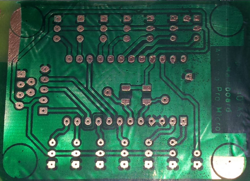
Here, the result: ignore all that is wrong with this picture (the borked test PCB, scratched from many tries; the wrinkles in the green material caused by the cellophane; the uneven spread; the fact that the clean bits are a bit misaligned and such). The rectangular areas are from tape used to fixate the printed mask cover. All of which can easily be remedied, now that the culprit is known.

enter image description here

As the process itself does not seem to be as wildly known as I assumed, here it is in my final form:

  • Clean the etched PCB as usual from any residue of the previous steps, including fingerprints etc.
  • Apply a small blob of the solder mask material ("10ml PCB UV Curable Solder Mask Repairing Paint Green") in the center.
  • Cover that with a very flexible plastic sheet - in my case cellophane, which is too flexible as it results in unsightly ripples in the final surface. Should not matter for the function. I will keep looking around for a little more stiff, but not too stiff, product. Avoid laser printer "transparent film / overhead" sheets as they are too stiff.
  • Use a credit card or whatever you have lying around to smooth out the initial blob of fluid across the whole surface.
  • Perform the usual UV development process that you already have in place for preparing the etch resistant photosensitive layer:
    • Lay your sheet of printed "solder mask mask" on top of it and fixate it with tape.
    • Weigh down with a sheet of glass.
    • Expose to UV for 5 minutes; I guess this is a spot where you have to experiment a bitminutes, depending on which lamp you use. Allegedly, you can use the sun, unless it is cloudy or night ;) , but as you should already have UV equipment, I don't see why.
  • Very carefully, and pulling sideways instead of up, remove the plastic sheet covering the mask.
  • Wipe off the uncured bits with ethanol and a soft brush.
  • Put back under UV for an hour or so to completely cure and harden the material.

Happy times, problem solved:

The issue was not, as helpfully suggested by @Sachin in the comments, the UV (lamp vs sun), age of material (> 1 year), duration of initial curing, but, also put forth by him, the type of plastic cover used in the process.

The final material I tried was simple household (kitchen) cellophane wrap - the very flimsy type that you use to wrap food in. Aside from the obvious tendency to wrinkle up, it came off trivially without damage, and the result is perfectly fine now. The mask that was not cured was easily brushed off with some ethanol.

Here, the result: ignore all that is wrong with this picture (the borked test PCB, scratched from many tries; the wrinkles in the green material caused by the cellophane; the uneven spread; the fact that the clean bits are a bit misaligned and such). The rectangular areas are from tape used to fixate the printed mask cover. All of which can easily be remedied, now that the culprit is known.

enter image description here

As the process itself does not seem to be as wildly known as I assumed, here it is in my final form:

  • Clean the etched PCB as usual from any residue of the previous steps, including fingerprints etc.
  • Apply a small blob of the solder mask material ("10ml PCB UV Curable Solder Mask Repairing Paint Green") in the center.
  • Cover that with a very flexible plastic sheet - in my case cellophane, which is too flexible as it results in unsightly ripples in the final surface. Should not matter for the function. I will keep looking around for a little more stiff, but not too stiff, product. Avoid laser printer "transparent film / overhead" sheets as they are too stiff.
  • Use a credit card or whatever you have lying around to smooth out the initial blob of fluid across the whole surface.
  • Perform the usual UV development process that you already have in place for preparing the etch resistant photosensitive layer:
    • Lay your sheet of printed "solder mask mask" on top of it and fixate it with tape.
    • Weigh down with a sheet of glass.
    • Expose to UV for 5 minutes; I guess this is a spot where you have to experiment a bit, depending on which lamp you use. Allegedly, you can use the sun, unless it is cloudy or night ;) , but as you should already have UV equipment, I don't see why.
  • Very carefully, and pulling sideways instead of up, remove the plastic sheet covering the mask.
  • Wipe off the uncured bits with ethanol and a soft brush.
  • Put back under UV for an hour or so to completely cure and harden the material.
Happy times, problem solved:

The issue was not, as helpfully suggested by @Sachin in the comments, the UV (lamp vs sun), age of material (> 1 year), duration of initial curing, but, also put forth by him, the type of plastic cover used in the process.

The final material I tried was simple household (kitchen) cellophane wrap - the very flimsy type that you use to wrap food in. Aside from the obvious tendency to wrinkle up, it came off trivially without damage, and the result is perfectly fine now. The mask that was not cured was easily brushed off with some ethanol.

Here, the result: ignore all that is wrong with this picture (the borked test PCB, scratched from many tries; the wrinkles in the green material caused by the cellophane; the uneven spread; the fact that the clean bits are a bit misaligned and such). The rectangular areas are from tape used to fixate the printed mask cover. All of which can easily be remedied, now that the culprit is known.

enter image description here

As the process itself does not seem to be as wildly known as I assumed, here it is in my final form:

  • Clean the etched PCB as usual from any residue of the previous steps, including fingerprints etc.
  • Apply a small blob of the solder mask material ("10ml PCB UV Curable Solder Mask Repairing Paint Green") in the center.
  • Cover that with a very flexible plastic sheet - in my case cellophane, which is too flexible as it results in unsightly ripples in the final surface. Should not matter for the function. I will keep looking around for a little more stiff, but not too stiff, product. Avoid laser printer "transparent film / overhead" sheets as they are too stiff.
  • Use a credit card or whatever you have lying around to smooth out the initial blob of fluid across the whole surface.
  • Perform the usual UV development process that you already have in place for preparing the etch resistant photosensitive layer:
    • Lay your sheet of printed "solder mask mask" on top of it and fixate it with tape.
    • Weigh down with a sheet of glass.
    • Expose to UV for 5 minutes, depending on which lamp you use.
  • Very carefully, and pulling sideways instead of up, remove the plastic sheet covering the mask.
  • Wipe off the uncured bits with ethanol and a soft brush.
  • Put back under UV for an hour or so to completely cure and harden the material.
deleted 63 characters in body
Source Link
AnoE
  • 508
  • 5
  • 15

Happy times, problem solved:

The issue was not, as helpfully suggested by @Sachin in the comments, the UV (lamp vs sun), age of material (> 1 year), duration of initial curing, but, also put forth by him, the type of plastic cover used in the process.

The final material I tried was simple household (kitchen) cellophane wrap - the very flimsy type that you use to wrap food in. Aside from the obvious tendency to wrinkle up, it came off trivially without damage, and the result is perfectly fine now. The mask that was not cured was easily brushed off with some ethanol.

Here, the result: ignore all that is wrong with this picture (the borked test PCB, scratched from many tries; the wrinkles in the green material caused by the cellophane,cellophane; the uneven spread,spread; the fact that the clean bits are a bit misaligned and such). The rectangular areas are from tape used to fixate the printed mask cover. All of which can easily be remedied, now that the culprit is known.

enter image description here

As the process itself does not seem to be as wildly known as I assumed, here it is in my final form:

  • Clean the etched PCB as usual from any residue of the previous steps, including fingerprints etc.
  • Apply a small blob of the solder mask material ("10ml PCB UV Curable Solder Mask Repairing Paint Green") in the center.
  • Cover that with a very flexible plastic sheet - in my case cellophane, which is too flexible as it results in unsightly ripples in the final surface. Should not matter for the function. I will keep looking around for a little more stiff, but not too stiff, product. Avoid laser printer "transparent film / overhead" sheets as they are too stiff.
  • Use a credit card or whatever you have lying around to smooth out the initial blob of fluid across the whole surface.
  • Perform the usual UV development process that you already have in place for preparing the etch resistant photosensitive layer:
    • Lay your sheet of printed "solder mask mask" on top of it and fixate it with some tape (outside of the PCB, obviously, not like in my test here).
    • Weigh down with a sheet of glass.
    • Expose to UV for 5 minutes; I guess this is a spot where you have to experiment a bit, depending on which lamp you use. Allegedly, you can use the sun, unless it is cloudy or night ;) , but as you should already have UV equipment, I don't see why not use it...
  • Very carefully, and pulling sideways instead of up, remove the plastic sheet covering the mask.
  • Wipe off the uncured bits with ethanol and a soft brush.
  • Put back under UV for an hour or so to completely cure and harden the material.

Happy times, problem solved:

The issue was not, as helpfully suggested by @Sachin in the comments, the UV (lamp vs sun), age of material (> 1 year), duration of initial curing, but, also put forth by him, the type of plastic cover used in the process.

The final material I tried was simple household (kitchen) cellophane wrap - the very flimsy type that you use to wrap food in. Aside from the obvious tendency to wrinkle up, it came off trivially without damage, and the result is perfectly fine now. The mask that was not cured was easily brushed off with some ethanol.

Here, the result: ignore all that is wrong with this picture (the borked test PCB, the wrinkles in the green material caused by the cellophane, the uneven spread, the fact that the clean bits are a bit misaligned and such). The rectangular areas are from tape used to fixate the printed mask cover. All of which can easily be remedied, now that the culprit is known.

enter image description here

As the process itself does not seem to be as wildly known as I assumed, here it is in my final form:

  • Clean the etched PCB as usual from any residue of the previous steps, including fingerprints etc.
  • Apply a small blob of the solder mask material ("10ml PCB UV Curable Solder Mask Repairing Paint Green") in the center.
  • Cover that with a very flexible plastic sheet - in my case cellophane, which is too flexible as it results in unsightly ripples in the final surface. Should not matter for the function. I will keep looking around for a little more stiff, but not too stiff, product. Avoid laser printer "transparent film / overhead" sheets as they are too stiff.
  • Use a credit card or whatever you have lying around to smooth out the initial blob of fluid across the whole surface.
  • Perform the usual UV development process that you already have in place for preparing the etch resistant photosensitive layer:
    • Lay your sheet of printed "solder mask mask" on top of it and fixate it with some tape (outside of the PCB, obviously, not like in my test here).
    • Weigh down with a sheet of glass.
    • Expose to UV for 5 minutes; I guess this is a spot where you have to experiment a bit, depending on which lamp you use. Allegedly, you can use the sun, but as you should already have UV equipment, why not use it...
  • Very carefully, and pulling sideways instead of up, remove the plastic sheet covering the mask.
  • Wipe off the uncured bits with ethanol and a soft brush.
  • Put back under UV for an hour or so to completely cure and harden the material.

Happy times, problem solved:

The issue was not, as helpfully suggested by @Sachin in the comments, the UV (lamp vs sun), age of material (> 1 year), duration of initial curing, but, also put forth by him, the type of plastic cover used in the process.

The final material I tried was simple household (kitchen) cellophane wrap - the very flimsy type that you use to wrap food in. Aside from the obvious tendency to wrinkle up, it came off trivially without damage, and the result is perfectly fine now. The mask that was not cured was easily brushed off with some ethanol.

Here, the result: ignore all that is wrong with this picture (the borked test PCB, scratched from many tries; the wrinkles in the green material caused by the cellophane; the uneven spread; the fact that the clean bits are a bit misaligned and such). The rectangular areas are from tape used to fixate the printed mask cover. All of which can easily be remedied, now that the culprit is known.

enter image description here

As the process itself does not seem to be as wildly known as I assumed, here it is in my final form:

  • Clean the etched PCB as usual from any residue of the previous steps, including fingerprints etc.
  • Apply a small blob of the solder mask material ("10ml PCB UV Curable Solder Mask Repairing Paint Green") in the center.
  • Cover that with a very flexible plastic sheet - in my case cellophane, which is too flexible as it results in unsightly ripples in the final surface. Should not matter for the function. I will keep looking around for a little more stiff, but not too stiff, product. Avoid laser printer "transparent film / overhead" sheets as they are too stiff.
  • Use a credit card or whatever you have lying around to smooth out the initial blob of fluid across the whole surface.
  • Perform the usual UV development process that you already have in place for preparing the etch resistant photosensitive layer:
    • Lay your sheet of printed "solder mask mask" on top of it and fixate it with tape.
    • Weigh down with a sheet of glass.
    • Expose to UV for 5 minutes; I guess this is a spot where you have to experiment a bit, depending on which lamp you use. Allegedly, you can use the sun, unless it is cloudy or night ;) , but as you should already have UV equipment, I don't see why.
  • Very carefully, and pulling sideways instead of up, remove the plastic sheet covering the mask.
  • Wipe off the uncured bits with ethanol and a soft brush.
  • Put back under UV for an hour or so to completely cure and harden the material.
Source Link
AnoE
  • 508
  • 5
  • 15

Happy times, problem solved:

The issue was not, as helpfully suggested by @Sachin in the comments, the UV (lamp vs sun), age of material (> 1 year), duration of initial curing, but, also put forth by him, the type of plastic cover used in the process.

The final material I tried was simple household (kitchen) cellophane wrap - the very flimsy type that you use to wrap food in. Aside from the obvious tendency to wrinkle up, it came off trivially without damage, and the result is perfectly fine now. The mask that was not cured was easily brushed off with some ethanol.

Here, the result: ignore all that is wrong with this picture (the borked test PCB, the wrinkles in the green material caused by the cellophane, the uneven spread, the fact that the clean bits are a bit misaligned and such). The rectangular areas are from tape used to fixate the printed mask cover. All of which can easily be remedied, now that the culprit is known.

enter image description here

As the process itself does not seem to be as wildly known as I assumed, here it is in my final form:

  • Clean the etched PCB as usual from any residue of the previous steps, including fingerprints etc.
  • Apply a small blob of the solder mask material ("10ml PCB UV Curable Solder Mask Repairing Paint Green") in the center.
  • Cover that with a very flexible plastic sheet - in my case cellophane, which is too flexible as it results in unsightly ripples in the final surface. Should not matter for the function. I will keep looking around for a little more stiff, but not too stiff, product. Avoid laser printer "transparent film / overhead" sheets as they are too stiff.
  • Use a credit card or whatever you have lying around to smooth out the initial blob of fluid across the whole surface.
  • Perform the usual UV development process that you already have in place for preparing the etch resistant photosensitive layer:
    • Lay your sheet of printed "solder mask mask" on top of it and fixate it with some tape (outside of the PCB, obviously, not like in my test here).
    • Weigh down with a sheet of glass.
    • Expose to UV for 5 minutes; I guess this is a spot where you have to experiment a bit, depending on which lamp you use. Allegedly, you can use the sun, but as you should already have UV equipment, why not use it...
  • Very carefully, and pulling sideways instead of up, remove the plastic sheet covering the mask.
  • Wipe off the uncured bits with ethanol and a soft brush.
  • Put back under UV for an hour or so to completely cure and harden the material.