My guess:
The reason is explained on the schematic. It says "AC return path for LCD MIPI which is referenced to VDD_MAIN".
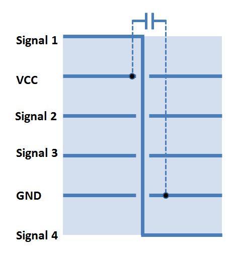
Most likely this means that some of the traces carrying fast MIPI signals use VDD as a reference plane. If these traces change reference planes to GND, for example through a via or a connector mating to a shielded flex, then caps between the two reference planes are required to allow the AC return current to find the shortest path and not wander around and cause EMI issues.
EDIT:
Say HF current flows into trace "Signal1". Return current will flow in the closest copper reference plane, here VCC. When the trace goes through a via, a stitching capacitor is added to allow the return current to also change layers. If both sides of the board had ground planes, a via would be enough.

