added 1769 characters in body
Source Link
Olin Lathrop
  • 315.1k
  • 36
  • 441
  • 928

There are a number of problems here:

  1. Draw the schematic with logical flow left to right. Fortunately what you have is simple enough to understand anyway, but it's still annoying to look at.
  2. You are clearly using Eagle, so there is no excuse for dumping screen shots on us. The different colors for nets and symbols and the little origin crosshairs for each component of the drawing have no relevance to us. They are something between you and your software, but inflicting them on others is rude and detracts from the message. Eagle has easy ways to export schematics to image files. Use them.
  3. Fix the orientation of text. There is no excuse for the R1 and R3 component designators to be rotated. There was plenty of room, and nothing stopping you from presenting the schematic properly. Don't be so lazy. Remember that you are asking volunteers for a favor.

I was going to get into circuit details, but I ran out of time. I gotta go now. Maybe I'll remember to come back later and talk about the circuit.

Added about the circuit

I see you have fixed the schematic, so now we can talk about the circuit.

You are essentially trying to use a common base configuration as a current sink. That's fine, except when the transistor doesn't get enough collector voltage, and too much of the emitter resistor current must come from the base. The circuit driving the base can't handle that.

One solution is more gain. During normal operation, that means there is less current drawn from the digital output, so any resistance in series with it causes less of a voltage drop. Here is one idea:

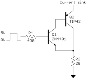
This still uses the same principle of a fixed base voltage on Q1 causing a fixed voltage across R2, which causes a fixed current to be sunk. The difference is the addition of Q2, which provides more current gain.

In this example, Q1 can be counted on to have a gain of 40, and Q2 of 30. The overall gain from the base current of Q1 to the collector current of Q2 is therefore at least 1200. The maximum Q1 base current during normal operation is therefore (150 mA)/1200 = 125 µA.

R2 is what it needs to be to cause about 150 mA at 4.3 V. R1 is then sized to limit the current when Q2 is unpowered. Since you didn't provide any specs, I arbitrarily picked 10 mA for the maximum safe current that the digital output can source.

Now we can work backwards and see what the error is due to R1. We know the maximum current thru R1 will be 125 µA, so the maximum voltage across it will be 54 mV. That amounts to a 2 mA error when reflected across R2, or about 1.3% of your 150 mA target. There are other larger sources of error here anyway, particularly the actual B-E voltage of Q1.

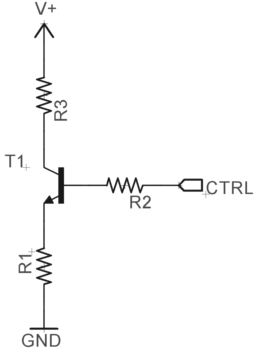
There are a number of problems here:

  1. Draw the schematic with logical flow left to right. Fortunately what you have is simple enough to understand anyway, but it's still annoying to look at.
  2. You are clearly using Eagle, so there is no excuse for dumping screen shots on us. The different colors for nets and symbols and the little origin crosshairs for each component of the drawing have no relevance to us. They are something between you and your software, but inflicting them on others is rude and detracts from the message. Eagle has easy ways to export schematics to image files. Use them.
  3. Fix the orientation of text. There is no excuse for the R1 and R3 component designators to be rotated. There was plenty of room, and nothing stopping you from presenting the schematic properly. Don't be so lazy. Remember that you are asking volunteers for a favor.

I was going to get into circuit details, but I ran out of time. I gotta go now. Maybe I'll remember to come back later and talk about the circuit.

Added about the circuit

I see you have fixed the schematic, so now we can talk about the circuit.

You are essentially trying to use a common base configuration as a current sink. That's fine, except when the transistor doesn't get enough collector voltage, and too much of the emitter resistor current must come from the base. The circuit driving the base can't handle that.

One solution is more gain. During normal operation, that means there is less current drawn from the digital output, so any resistance in series with it causes less of a voltage drop. Here is one idea:

This still uses the same principle of a fixed base voltage on Q1 causing a fixed voltage across R2, which causes a fixed current to be sunk. The difference is the addition of Q2, which provides more current gain.

In this example, Q1 can be counted on to have a gain of 40, and Q2 of 30. The overall gain from the base current of Q1 to the collector current of Q2 is therefore at least 1200. The maximum Q1 base current during normal operation is therefore (150 mA)/1200 = 125 µA.

R2 is what it needs to be to cause about 150 mA at 4.3 V. R1 is then sized to limit the current when Q2 is unpowered. Since you didn't provide any specs, I arbitrarily picked 10 mA for the maximum safe current that the digital output can source.

Now we can work backwards and see what the error is due to R1. We know the maximum current thru R1 will be 125 µA, so the maximum voltage across it will be 54 mV. That amounts to a 2 mA error when reflected across R2, or about 1.3% of your 150 mA target. There are other larger sources of error here anyway, particularly the actual B-E voltage of Q1.
Source Link
Olin Lathrop
  • 315.1k
  • 36
  • 441
  • 928

There are a number of problems here:

  1. Draw the schematic with logical flow left to right. Fortunately what you have is simple enough to understand anyway, but it's still annoying to look at.
  2. You are clearly using Eagle, so there is no excuse for dumping screen shots on us. The different colors for nets and symbols and the little origin crosshairs for each component of the drawing have no relevance to us. They are something between you and your software, but inflicting them on others is rude and detracts from the message. Eagle has easy ways to export schematics to image files. Use them.
  3. Fix the orientation of text. There is no excuse for the R1 and R3 component designators to be rotated. There was plenty of room, and nothing stopping you from presenting the schematic properly. Don't be so lazy. Remember that you are asking volunteers for a favor.

I was going to get into circuit details, but I ran out of time. I gotta go now. Maybe I'll remember to come back later and talk about the circuit.