Would these wires be considered a "trace", "jump", a "via", or something else entirely?
Usually jumper wires or wire links.
How would this be illustrated on a schematic to indicate that it is an actual wire and not part of the etching?
They would not normally be shown on a schematic because they don't affect circuit operation and the use of the links is decided by the person who does the PCB layout. If, for some reason, they have to be shown on the schematic a 0 Ω resistor could be used.
If one were to purchase this kind of solid wire, what would its gauge be, its material, and how would I search for it so that I exclude results with shielding?
Gauge could be determined by PCB drill size for standardisation, bending equipment capability, current handling capacity, etc. Plated copper would be the normal choice for good conductivity and ability to solder.
Are there any issues with running wires like this without shielding? Such as electrical interference.
No. They're used here because the board is single sided. All the traces are unshielded.
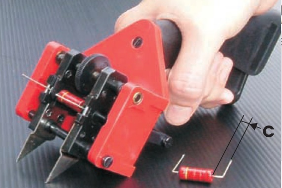
Unless I am mistaken, these do not appear to be hand-made due do their exactness and how straight they are. How does a machine place these? Or are they pre-bent, placed, and then sent through a wave solder machine?
Given the few and odd components this board is most likely to be hand assembled.
Figure 1. An axial-lead component former would probably do the job. Source: OLAMEF USA.
When would this method still used today? Or is it something that is an artifact of single-layer boards where one would otherwise use a through-hole via and traces on the other side?
Yes, definitely, maybe, no. It depends. If it solves a particular routing problem, avoids an extra layer, etc., then why not.
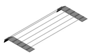
Figure 2. Vishay make jumper wire taped in ammo fashion for ease of use in automatic insertion equipment. See Vishay WIRE0580000000A500 datasheet.


