Bumped by Community user
Formatted list
Source Link
JYelton
  • 34.9k
  • 34
  • 147
  • 272

Questions on using Using a fully differential amplifier as a differential ADC driver

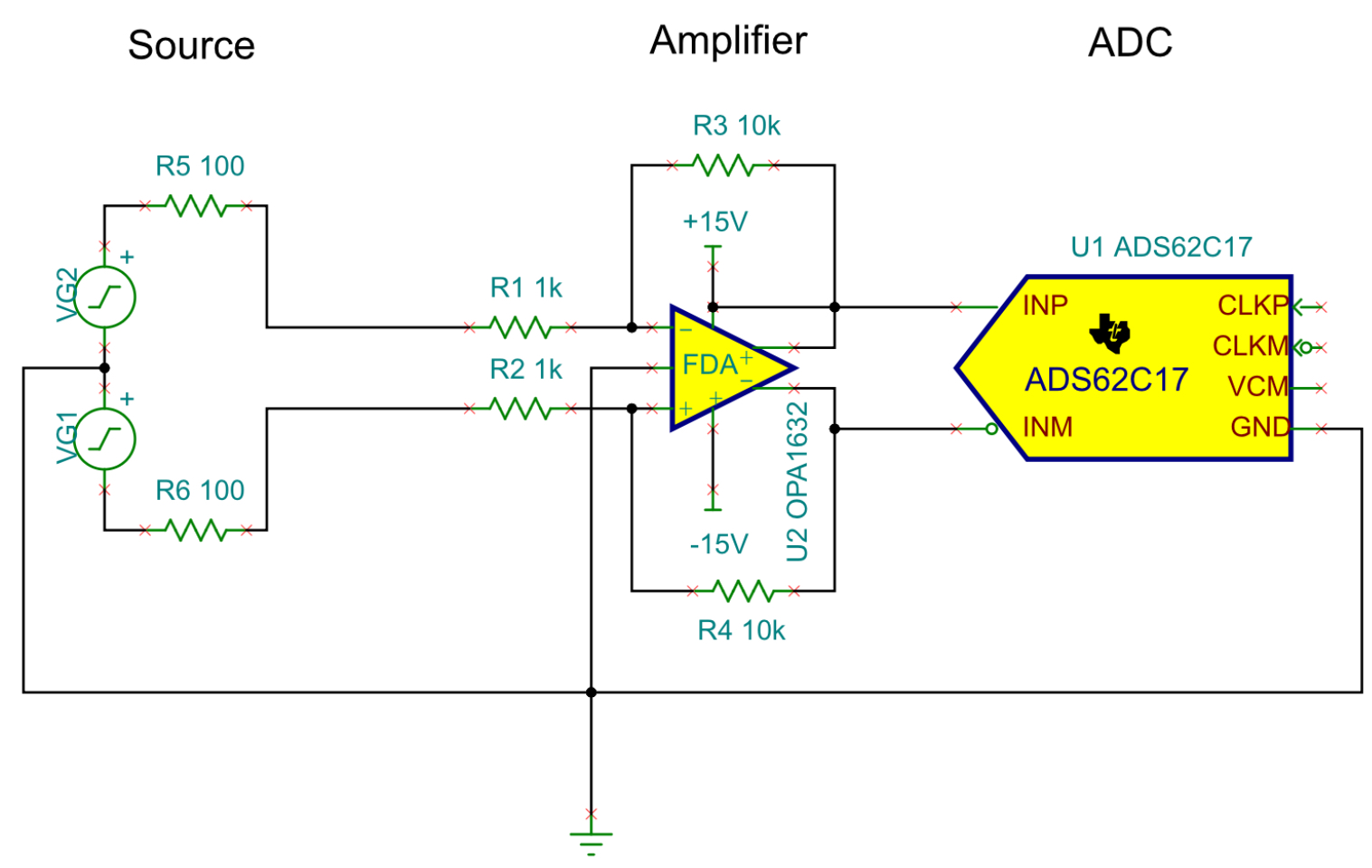
Regarding my previous question, I decided to use a “fully differential amplifier” to obtain a voltage gain of 10. The source and ADC are also differential. The source is unipolar and its output resistance is given as 100 Ohm. I want to amplify the +/-200mV source voltage by gain of 10 or more. ADC input can be set to +/-5V or +/-10V. Below I have drawn the schematics:

enter image description here

Above ADC and the amplifier are just representative. ADC is actually a channel of a differential ended data acquisition board. OPA 1632 represents a fully differential amplifier but it is designed for audio. My freq of interest is not audio, it is actually DC to 150Hz and need low noise as possible.

If this topology is correct, before I start to build this I noticed I have some inexperience about some critical decision.

I summerizedsummarized the questions for clarity:

  1. I want to use 5 meters of STP cable between the source and ADC. Should the amplifier be right after the source or right before the ADC?

  2. As far as I understand the voltage gain is 1+R3/R1 = 1+R4/R2 where R3=R4 and R1=R2. But what values of resistors are reasonable?

  3. R1, R2, R3 and R4 will have tolerances. In that case how can matched resistor arrays be configured to obtain better CM noise immunity?

(Schematic does not show an anti-aliasing filter)

Questions on using a fully differential amplifier as a differential ADC driver

Regarding my previous question, I decided to use a “fully differential amplifier” to obtain a voltage gain of 10. The source and ADC are also differential. The source is unipolar and its output resistance is given as 100 Ohm. I want to amplify the +/-200mV source voltage by gain of 10 or more. ADC input can be set to +/-5V or +/-10V. Below I have drawn the schematics:

enter image description here

Above ADC and the amplifier are just representative. ADC is actually a channel of a differential ended data acquisition board. OPA 1632 represents a fully differential amplifier but it is designed for audio. My freq of interest is not audio, it is actually DC to 150Hz and need low noise as possible.

If this topology is correct, before I start to build this I noticed I have some inexperience about some critical decision.

I summerized the questions for clarity:

  1. I want to use 5 meters of STP cable between the source and ADC. Should the amplifier be right after the source or right before the ADC?

  2. As far as I understand the voltage gain is 1+R3/R1 = 1+R4/R2 where R3=R4 and R1=R2. But what values of resistors are reasonable?

  3. R1, R2, R3 and R4 will have tolerances. In that case how can matched resistor arrays be configured to obtain better CM noise immunity?

(Schematic does not show an anti-aliasing filter)

Using a fully differential amplifier as a differential ADC driver

Regarding my previous question, I decided to use a “fully differential amplifier” to obtain a voltage gain of 10. The source and ADC are also differential. The source is unipolar and its output resistance is given as 100 Ohm. I want to amplify the +/-200mV source voltage by gain of 10 or more. ADC input can be set to +/-5V or +/-10V. Below I have drawn the schematics:

enter image description here

Above ADC and the amplifier are just representative. ADC is actually a channel of a differential ended data acquisition board. OPA 1632 represents a fully differential amplifier but it is designed for audio. My freq of interest is not audio, it is actually DC to 150Hz and need low noise as possible.

If this topology is correct, before I start to build this I noticed I have some inexperience about some critical decision.

I summarized the questions for clarity:

  1. I want to use 5 meters of STP cable between the source and ADC. Should the amplifier be right after the source or right before the ADC?

  2. As far as I understand the voltage gain is 1+R3/R1 = 1+R4/R2 where R3=R4 and R1=R2. But what values of resistors are reasonable?

  3. R1, R2, R3 and R4 will have tolerances. In that case how can matched resistor arrays be configured to obtain better CM noise immunity?

(Schematic does not show an anti-aliasing filter)
edited body
Source Link
user1999
  • 1.5k
  • 5
  • 26
  • 36

Questions on using a fully differential amplifier as ana differential ADC driver

Regarding my previous question, I decided to use a “fully differential amplifier” to obtain a voltage gain of 10. The source and ADC are also differential. The source is unipolar and its output resistance is given as 100 Ohm. I want to amplify the +/-200mV source voltage by gain of 10 or more. ADC input can be set to +/-5V or +/-10V. Below I have drawn the schematics:

enter image description hereenter image description here

Above ADC and the amplifier are just representative. ADC is actually a channel of a differential ended data acquisition board. OPA 1632 represents a fully differential amplifier but it is designed for audio. My freq of interest is not audio, it is actually DC to 150Hz and need low noise as possible.

If this topology is correct, before I start to build this I noticed I have some inexperience about some critical decision.

I summerized the questions for clarity:

  1. I want to use 5 meters of STP cable between the source and ADC. Should the amplifier be right after the source or right before the ADC?

  2. As far as I understand the voltage gain is 1+R3/R1 = 1+R4/R2 where R3=R4 and R1=R2. But what values of resistors are reasonable?

  3. R1, R2, R3 and R4 will have tolerances. In that case how can matched resistor arrays be configured to obtain better CM noise immunity?

(Schematic does not show an anti-aliasing filter)

Questions on using a fully differential amplifier as an differential ADC driver

Regarding my previous question, I decided to use a “fully differential amplifier” to obtain a voltage gain of 10. The source and ADC are also differential. The source is unipolar and its output resistance is given as 100 Ohm. I want to amplify the +/-200mV source voltage by gain of 10 or more. ADC input can be set to +/-5V or +/-10V. Below I have drawn the schematics:

enter image description here

Above ADC and the amplifier are just representative. ADC is actually a channel of a differential ended data acquisition board. OPA 1632 represents a fully differential amplifier but it is designed for audio. My freq of interest is not audio, it is actually DC to 150Hz and need low noise as possible.

If this topology is correct, before I start to build this I noticed I have some inexperience about some critical decision.

I summerized the questions for clarity:

  1. I want to use 5 meters of STP cable between the source and ADC. Should the amplifier be right after the source or right before the ADC?

  2. As far as I understand the voltage gain is 1+R3/R1 = 1+R4/R2 where R3=R4 and R1=R2. But what values of resistors are reasonable?

  3. R1, R2, R3 and R4 will have tolerances. In that case how can matched resistor arrays be configured to obtain better CM noise immunity?

(Schematic does not show an anti-aliasing filter)

Questions on using a fully differential amplifier as a differential ADC driver

Regarding my previous question, I decided to use a “fully differential amplifier” to obtain a voltage gain of 10. The source and ADC are also differential. The source is unipolar and its output resistance is given as 100 Ohm. I want to amplify the +/-200mV source voltage by gain of 10 or more. ADC input can be set to +/-5V or +/-10V. Below I have drawn the schematics:

enter image description here

Above ADC and the amplifier are just representative. ADC is actually a channel of a differential ended data acquisition board. OPA 1632 represents a fully differential amplifier but it is designed for audio. My freq of interest is not audio, it is actually DC to 150Hz and need low noise as possible.

If this topology is correct, before I start to build this I noticed I have some inexperience about some critical decision.

I summerized the questions for clarity:

  1. I want to use 5 meters of STP cable between the source and ADC. Should the amplifier be right after the source or right before the ADC?

  2. As far as I understand the voltage gain is 1+R3/R1 = 1+R4/R2 where R3=R4 and R1=R2. But what values of resistors are reasonable?

  3. R1, R2, R3 and R4 will have tolerances. In that case how can matched resistor arrays be configured to obtain better CM noise immunity?

(Schematic does not show an anti-aliasing filter)

added 53 characters in body
Source Link
user1999
  • 1.5k
  • 5
  • 26
  • 36

Regarding my previous question, I decided to use a “fully differential amplifier” to obtain a voltage gain of 10. The source and ADC are also differential. The source is unipolar and its output resistance is given as 100 Ohm. I want to amplify the +/-200mV source voltage by gain of 10 or more. ADC input can be set to +/-5V or +/-10V. Below I have drawn the schematics:

enter image description here

Above ADC and the amplifier are just representative. ADC is actually a channel of a differential ended data acquisition board. OPA 1632 represents a fully differential amplifier but it is designed for audio. My freq of interest is not audio, it is actually DC to 150Hz and need low noise as possible.

If this topology is correct, before I start to build this I noticed I have some inexperience about some critical decision.

I summerized the questions for clarity:

  1. I want to use 5 meters of STP cable between the source and ADC. Should the amplifier be right after the source or right before the ADC?

  2. As far as I understand the voltage gain is 1+R3/R1 = 1+R4/R2 where R3=R4 and R1=R2. But what values of resistors are reasonable?

  3. R1, R2, R3 and R4 will have tolerances. In that case how can matched resistor arrays be configured to obtain better CM noise immunity?

(Schematic does not show an anti-aliasing filter)

Regarding my previous question, I decided to use a “fully differential amplifier” to obtain a voltage gain of 10. The source and ADC are also differential. The source is unipolar and its output resistance is given as 100 Ohm. I want to amplify the +/-200mV source voltage by gain of 10 or more. ADC input can be set to +/-5V or +/-10V. Below I have drawn the schematics:

enter image description here

Above ADC and the amplifier are just representative. ADC is actually a channel of a differential ended data acquisition board. OPA 1632 represents a fully differential amplifier but it is designed for audio. My freq of interest is not audio, it is actually DC to 150Hz and need low noise as possible.

If this topology is correct, before I start to build this I noticed I have some inexperience about some critical decision.

I summerized the questions for clarity:

  1. I want to use 5 meters of STP cable between the source and ADC. Should the amplifier be right after the source or right before the ADC?

  2. As far as I understand the voltage gain is 1+R3/R1 = 1+R4/R2 where R3=R4 and R1=R2. But what values of resistors are reasonable?

  3. R1, R2, R3 and R4 will have tolerances. In that case how can matched resistor arrays be configured to obtain better CM noise immunity?

(Schematic does not show an anti-aliasing filter)

Source Link
user1999
  • 1.5k
  • 5
  • 26
  • 36
Loading