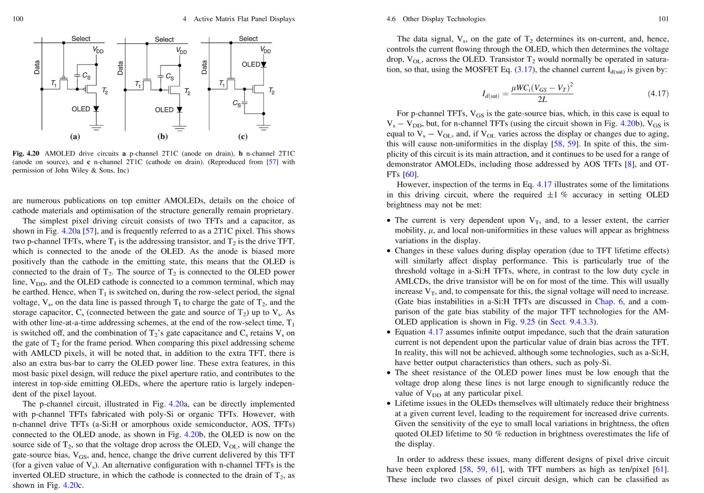
My question stems from OLED pixel circuitswas incorrectly posed, where it is said that the LED must be loaded ontobecause I didn't include the drain side ofcapacitor connecting the transistor in series to prevent non-uniformity of brightness duegate to non-uniformityone of diode parasitic series resistance (or variation in threshold voltage perhaps).So it is said that if the diode is to be placed between the transistor and ground, the transistor should be a p-type transistor, such that the source voltage is connected to power source. If an n-type transistor is used, the LED should be placed in between the power source and the drain side, such that the source is now connected to ground.
These are thin-film transistors, so I don't believe there is any fourth terminal.
So why does So in fact this matter? Thinking of the OLED as a resistor, who cares if the resistorquestion is placed onregarding common source orvs common drain side -- regardless the overall electric field across channel, and the average electric field between the channel and the gate is the same. What am I missing here? Is there some unexplained fourth terminal even though the transistor is on an insulating substrate? Every explanation of this either gives circular logic ("transistor current is dependent on Vgs"..comparison.ok, why? why not Vgd?) or it incorporates the body terminal into the situation (so it doesn't matter on insulating substrate? B/c text book implies it still matters). Is there any explanation that doesn't incorporate a fourth terminal, and if not, please explain clearly what exactly this fourth terminal would be on an insulating substrate.
It has been difficult for people to understand this question, here is the circuit:

