EDIT how to design the circuit.
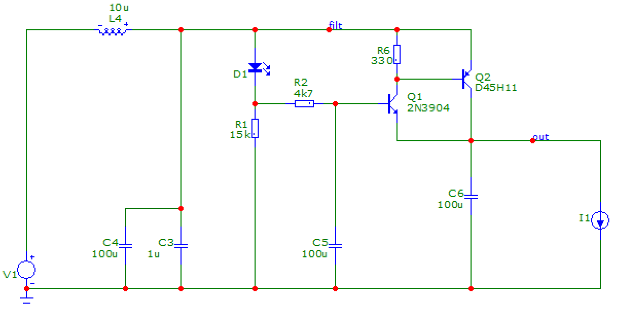
You specified a max current of 0.5A and max voltage 30V. First we need a power transistor for Q2, it should handle the voltage, current, power and safe operating area. With 2-3V dropout at 0.5A it will dissipate less than 2W, so let's use a TO220 or DPAK package.
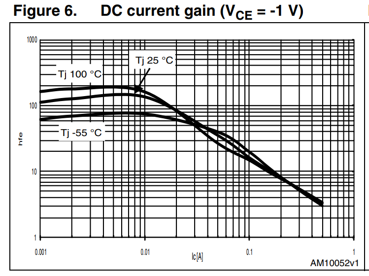
Q1 provides Q2's base current, and Q1 is not a power transistor, so we don't want Q1 to run at more than say 10-20mA for 500mA output, which means Q2 should have at least hFe>25 at 0.5A. The STN9260 you have won't work, as its hFe vs Ic curve shows, at 500mA hFe drops too much.
So let's use TIP127 instead, it's a darlington so it will have plenty of gain, plus I have the Spice model. Datasheet says minimum hFe around 1000, so its base current will be less than 0.5mA. Q1's Ic is S2's Ib plus 2mA from R6. So, Q1's base current will be less than 20µA, which means we can set R2=4k7 for an entirely arbitrary 100mV drop on R2...
Q1's base sees an impedance of C5 in parallel with (R2+D1) ; in this case R1 is irrelevant as D1 is ON, its dynamic impedance will be a few omhs to a few tens of ohms. So at DC R2 dominates the impedance seen by Q2's base.
Q2 Vce is D1's Vf plus Q1 Vbe. If D1 is a red LED, its Vf will be 1.6-1.8V so we get 2.2-2.4V for Q2 Vce, that should work fine. You can use a green LED for an extra 0.2-0.4V.
On power up, C5 will require a few seconds to charge through R2.
In case of short circuit at the output, C5 will discharge through Q1's base into the output. In order to avoid excessive base current, it would be a good idea to add a 100R base resistor to Q1 that I forgot in the above schematic.


