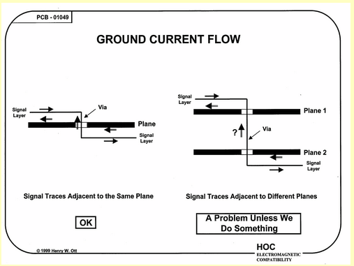
NoOOoooOOoOoooo. That's such a waste of a 4-layer PCB! Please find another approach than shorting two adjacent planes together to turn a very useful 4-layer PCB into effectively what is a 3-layer PCB.
Should you go with this highly unrecommended approachThat aside, there is an issue (whichalso called a method called via fencing. It is like a ground ring, except in 3 dimensions where you tie parallel ground traces on layers above and below the signal trace with tightly spaced vias.
There is also anpotential issue ifwhich can arise whenever you have multiple planes of any kind, even planes of different kinds). It is called changing reference planes. It is related to the fact that high frequency currents cannot flow through the copper plane due to the skin effect. They can only flow from one side of a plane to the other around the edges such(such as the edgeedges of via holes which your GND-GNDcutouts formed by signal traces as they pass through a plane pair might not have depending on how you lay things out).
Taken from: http://www.hottconsultants.com/techtips/pcb-stack-up-6.html
This is usually alleviated by placing ground vias near any signal via that passes through the plane, in order to provide a nearby edge for the return currents to cross from one side of the plane to the other.
But seriously, just read that entire link. The only reason I post the picture here is so the answer remains useful if the link ever gets broken.

