Became Hot Network Question
added 4 characters in body
Source Link
jrive
  • 639
  • 4
  • 16

So how negative can I drive the Vgs of an N-channel Mosfet before damage occurs? Datasheets specify BVDSS and BVGSS but these are "forward" breakdown voltages -- ie the absolute maximum Vds before avalanche breakdown of the drain body pn junction, and the maximum gate drive voltage before the electric field breaks down the gate oxide. I can't find the "negative" breakdown voltages in the device specifications.

Does the susceptibility of the gate oxide to an excessive e-field then suggest that the maximum "negative" Vgs is the same as the BVGSS specified but in the opposite polarity?

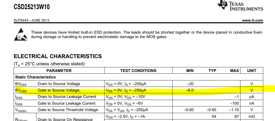
EDIT: Here's a portion of the p-channel device I was looking at that prompted the question: enter image description here
So how negative can I drive the Vgs of an N-channel Mosfet before damage occurs? Datasheets specify BVDSS and BVGSS but these are "forward" breakdown voltages -- ie the absolute maximum Vds before avalanche breakdown of the drain body pn junction, and the maximum gate drive voltage before the electric field breaks down the gate oxide. I can't find the "negative" breakdown voltages in the device specifications.

Does the susceptibility of gate oxide to an excessive e-field then suggest that the maximum "negative" Vgs is the same as the BVGSS specified but in the opposite polarity?

EDIT: Here's a portion of the p-channel device I was looking at that prompted the question: enter image description here

So how negative can I drive the Vgs of an N-channel Mosfet before damage occurs? Datasheets specify BVDSS and BVGSS but these are "forward" breakdown voltages -- ie the absolute maximum Vds before avalanche breakdown of the drain body pn junction, and the maximum gate drive voltage before the electric field breaks down the gate oxide. I can't find the "negative" breakdown voltages in the device specifications.

Does the susceptibility of the gate oxide to an excessive e-field then suggest that the maximum "negative" Vgs is the same as the BVGSS specified but in the opposite polarity?

EDIT: Here's a portion of the p-channel device I was looking at that prompted the question: enter image description here

typo
Source Link
jrive
  • 639
  • 4
  • 16

So how negative can I drive the Vgs of an N-channel Mosfet before damage occurs? Datasheets specify BVDSS and BVGSS but these are "forward" breakdown voltages -- ie the absolute maximum Vds before avalanche breakdown of the drain body pn junction, and the maximum gate drive voltage before the electric field breaks down the gate oxide. I can't find the "negative" breakdown voltages in the device specifications.

Does the susceptibility of gate oxide to an excessive e-field then suggest that the maximum "negative" Vgs is the same as the BVGSS specified but in the opposite polarity?

EDIT: Here's a portion of the p-channel device I was looking at thethat prompted the question: enter image description here

So how negative can I drive the Vgs of an N-channel Mosfet before damage occurs? Datasheets specify BVDSS and BVGSS but these are "forward" breakdown voltages -- ie the absolute maximum Vds before avalanche breakdown of the drain body pn junction, and the maximum gate drive voltage before the electric field breaks down the gate oxide. I can't find the "negative" breakdown voltages in the device specifications.

Does the susceptibility of gate oxide to an excessive e-field then suggest that the maximum "negative" Vgs is the same as the BVGSS specified but in the opposite polarity?

EDIT: Here's a portion of the p-channel device I was looking at the prompted the question: enter image description here

So how negative can I drive the Vgs of an N-channel Mosfet before damage occurs? Datasheets specify BVDSS and BVGSS but these are "forward" breakdown voltages -- ie the absolute maximum Vds before avalanche breakdown of the drain body pn junction, and the maximum gate drive voltage before the electric field breaks down the gate oxide. I can't find the "negative" breakdown voltages in the device specifications.

Does the susceptibility of gate oxide to an excessive e-field then suggest that the maximum "negative" Vgs is the same as the BVGSS specified but in the opposite polarity?

EDIT: Here's a portion of the p-channel device I was looking at that prompted the question: enter image description here

added portion of datasheet of device
Source Link
jrive
  • 639
  • 4
  • 16

So how negative can I drive the Vgs of an N-channel Mosfet before damage occurs? Datasheets specify BVDSS and BVGSS but these are "forward" breakdown voltages -- ie the absolute maximum Vds before avalanche breakdown of the drain body pn junction, and the maximum gate drive voltage before the electric field breaks down the gate oxide. I can't find the "negative" breakdown voltages in the device specifications.

Does the susceptibility of gate oxide to an excessive e-field then suggest that the maximum "negative" Vgs is the same as the BVGSS specified but in the opposite polarity?

EDIT: Here's a portion of the p-channel device I was looking at the prompted the question: enter image description here

So how negative can I drive the Vgs of an N-channel Mosfet before damage occurs? Datasheets specify BVDSS and BVGSS but these are "forward" breakdown voltages -- ie the absolute maximum Vds before avalanche breakdown of the drain body pn junction, and the maximum gate drive voltage before the electric field breaks down the gate oxide. I can't find the "negative" breakdown voltages in the device specifications.

Does the susceptibility of gate oxide to an excessive e-field then suggest that the maximum "negative" Vgs is the same as the BVGSS specified but in the opposite polarity?

EDIT: Here's a portion of the p-channel device I was looking at the prompted the question: enter image description here

Source Link
jrive
  • 639
  • 4
  • 16
Loading