When I started learning CMOS analog IC design I had many similar questions. Your circuit is from Razavi. It is rather to explain amplification properties of CMOS transistors:

enter image description hereenter image description here

SourceAbove picture is from: forum https://ocw.mit.edu/courses/electrical-engineering-and-computer-science/6-012-microelectronic-devices-and-circuits-fall-2005/lecture-notes/lecture19annotat.pdf

Please read it.allaboutcircuits You have a lot explained there.com

In your picture the input signal Vin is on the gate while the output signal is created on the Rd resistor. Depending what is your Vin DC voltage and Vin AC voltage you will get different Vout output signal.

In my opinion, the best thing you can do is not to stop for a long time on such things and go ahead and read and learn more. I recommend you Baker or Camenzind. The more circuits you meet, the more you understand and learn. Then it starts to be simple and obvious. For example take a look on the full circuit:
enter image description here Source: https://payhip.com/b/5Srt ("Preview" button in right top corner)

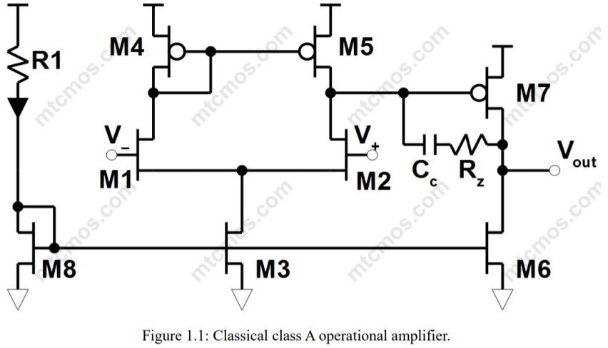
M3 and M6 transistors are biased by M8 transistor (current mirrors). Your case is similar to M7 transistor, which instead the resistor Rd has M6 transistor on its output. M6 works as a current source so it is seen as a big resistor. The DC voltage on M7 gate is set by M4-M5 current mirror. Then only AC signal is generated when V- and V+ signals start to be different.

When I started learning CMOS analog IC design I had many similar questions. Your circuit is from Razavi. It is rather to explain amplification properties of CMOS transistors:

enter image description here

Source: forum.allaboutcircuits.com

In your picture the input signal Vin is on the gate while the output signal is created on the Rd resistor. Depending what is your Vin DC voltage and Vin AC voltage you will get different Vout output signal.

In my opinion, the best thing you can do is not to stop for a long time on such things and go ahead and read and learn more. I recommend you Baker or Camenzind. The more circuits you meet, the more you understand and learn. Then it starts to be simple and obvious. For example take a look on the full circuit:

enter image description here Source: https://payhip.com/b/5Srt ("Preview" button in right top corner)

M3 and M6 transistors are biased by M8 transistor (current mirrors). Your case is similar to M7 transistor, which instead the resistor Rd has M6 transistor on its output. M6 works as a current source so it is seen as a big resistor. The DC voltage on M7 gate is set by M4-M5 current mirror. Then only AC signal is generated when V- and V+ signals start to be different.
When I started learning CMOS analog IC design I had many similar questions. Your circuit is from Razavi. It is rather to explain amplification properties of CMOS transistors:

enter image description here

Above picture is from: https://ocw.mit.edu/courses/electrical-engineering-and-computer-science/6-012-microelectronic-devices-and-circuits-fall-2005/lecture-notes/lecture19annotat.pdf

Please read it. You have a lot explained there.

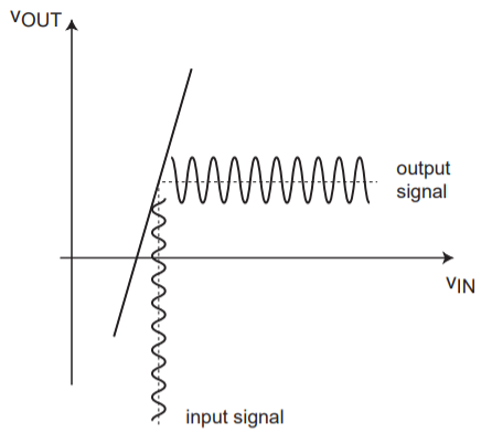
In your picture the input signal Vin is on the gate while the output signal is created on the Rd resistor. Depending what is your Vin DC voltage and Vin AC voltage you will get different Vout output signal.

In my opinion, the best thing you can do is not to stop for a long time on such things and go ahead and read and learn more. I recommend you Baker or Camenzind. The more circuits you meet, the more you understand and learn. Then it starts to be simple and obvious. For example take a look on the full circuit:

enter image description here Source: https://payhip.com/b/5Srt ("Preview" button in right top corner)

M3 and M6 transistors are biased by M8 transistor (current mirrors). Your case is similar to M7 transistor, which instead the resistor Rd has M6 transistor on its output. M6 works as a current source so it is seen as a big resistor. The DC voltage on M7 gate is set by M4-M5 current mirror. Then only AC signal is generated when V- and V+ signals start to be different.

Source Link
Tako
  • 194
  • 10

When I started learning CMOS analog IC design I had many similar questions. Your circuit is from Razavi. It is rather to explain amplification properties of CMOS transistors:

enter image description here

Source: forum.allaboutcircuits.com

In your picture the input signal Vin is on the gate while the output signal is created on the Rd resistor. Depending what is your Vin DC voltage and Vin AC voltage you will get different Vout output signal.

In my opinion, the best thing you can do is not to stop for a long time on such things and go ahead and read and learn more. I recommend you Baker or Camenzind. The more circuits you meet, the more you understand and learn. Then it starts to be simple and obvious. For example take a look on the full circuit:

enter image description here Source: https://payhip.com/b/5Srt ("Preview" button in right top corner)

M3 and M6 transistors are biased by M8 transistor (current mirrors). Your case is similar to M7 transistor, which instead the resistor Rd has M6 transistor on its output. M6 works as a current source so it is seen as a big resistor. The DC voltage on M7 gate is set by M4-M5 current mirror. Then only AC signal is generated when V- and V+ signals start to be different.