add schematic
Source Link
Dave Tweed
  • 178.3k
  • 17
  • 242
  • 418

There are many problems with this design.

First of all, do you really think you can maintain 50 dB of isolation with the two connectors right next to each other like that? Attenuators are generally built in straight lines for a reason, not folded around like that.

Second of all, the design of your pi-network attenuators looks fine, but you can't simply connect a couple of 100 Ω resistors across the input like that. Your resistors "1", "2" and "At1.1" are all in parallel — you need to make sure that the resistance of this parallel combination is 61.11 Ω, which would mean using two 121 Ω resistors or maybe four 243 Ω resistors.

Together, those resistors will be dissipating 80% of the input power, while the entire rest of the attenuator (mainly "At1.2", "At1.3" and "At1.4") will be dissipating only 20% of the input power. You can probably use fewer resistors here.


As far as the trace width goes as well as the overall layout, there's no reason not to combine parallel resistors after the first stage, and you shouldn't use stubs to connect them to the signal path — just merge the pads directly with the trace.

And unless you're trying to use this in the tens of GHz range, the trace lengths are too short to worry much about exact impedances anyway — the parasitics associated with the pads and the components themselves are going to overwhelm any matching issues.


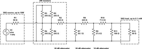
Here's the final design, using E96 resistor values. The theoretical values for 50 Ω attenuators (calculated here) are:

  • 20 dB: 61.11 Ω shunt, 247.5 Ω series
  • 10 dB: 96.25 Ω shunt, 71.15 Ω series

schematic

simulate this circuit – Schematic created using CircuitLab

I would arrange R3-R6 symmetrically around the input connector, keeping the current path loops as short as physically possible. Together, R2-R6 dissipate 99% of the input power, leaving just 100 mW that mostly goes into R7 (whose value is the parallel combination of two 61.11 Ω resistors).

There are many problems with this design.

First of all, do you really think you can maintain 50 dB of isolation with the two connectors right next to each other like that? Attenuators are generally built in straight lines for a reason, not folded around like that.

Second of all, the design of your pi-network attenuators looks fine, but you can't simply connect a couple of 100 Ω resistors across the input like that. Your resistors "1", "2" and "At1.1" are all in parallel — you need to make sure that the resistance of this parallel combination is 61.11 Ω, which would mean using two 121 Ω resistors or maybe four 243 Ω resistors.

Together, those resistors will be dissipating 80% of the input power, while the entire rest of the attenuator (mainly "At1.2", "At1.3" and "At1.4") will be dissipating only 20% of the input power. You can probably use fewer resistors here.


As far as the trace width goes as well as the overall layout, there's no reason not to combine parallel resistors after the first stage, and you shouldn't use stubs to connect them to the signal path — just merge the pads directly with the trace.

And unless you're trying to use this in the tens of GHz range, the trace lengths are too short to worry much about exact impedances anyway — the parasitics associated with the pads and the components themselves are going to overwhelm any matching issues.


Here's the final design, using E96 resistor values. The theoretical values for 50 Ω attenuators (calculated here) are:

  • 20 dB: 61.11 Ω shunt, 247.5 Ω series
  • 10 dB: 96.25 Ω shunt, 71.15 Ω series

schematic

simulate this circuit – Schematic created using CircuitLab

I would arrange R3-R6 symmetrically around the input connector, keeping the current path loops as short as physically possible. Together, R2-R6 dissipate 99% of the input power, leaving just 100 mW that mostly goes into R7 (whose value is the parallel combination of two 61.11 Ω resistors).

added 527 characters in body
Source Link
Dave Tweed
  • 178.3k
  • 17
  • 242
  • 418

There are many problems with this design.

First of all, do you really think you can maintain 50 dB of isolation with the two connectors right next to each other like that? Attenuators are generally built in straight lines for a reason, not folded around like that.

Second of all, the design of your pi-network attenuators looks fine, but you can't simply connect a couple of 100 Ω resistors across the input like that. Your resistors "1", "2" and "At1.1" are all in parallel — you need to make sure that the resistance of this parallel combination is 61.11 Ω, which would mean using two 121 Ω resistors or maybe four 243 Ω resistors.

Together, those resistors will be dissipating 80% of the input power, while the entire rest of the attenuator (mainly "At1.2", "At1.3" and "At1.4") will be dissipating only 20% of the input power. You can probably use fewer resistors here.


As far as the trace width goes as well as the overall layout, there's no reason not to combine parallel resistors after the first stage, and you shouldn't use stubs to connect them to the signal path — just merge the pads directly with the trace.

And unless you're trying to use this in the tens of GHz range, the trace lengths are too short to worry much about exact impedances anyway — the parasitics associated with the pads and the components themselves are going to overwhelm any matching issues.

There are many problems with this design.

First of all, do you really think you can maintain 50 dB of isolation with the two connectors right next to each other like that? Attenuators are generally built in straight lines for a reason, not folded around like that.

Second of all, the design of your pi-network attenuators looks fine, but you can't simply connect a couple of 100 Ω resistors across the input like that. Your resistors "1", "2" and "At1.1" are all in parallel — you need to make sure that the resistance of this parallel combination is 61.11 Ω, which would mean using two 121 Ω resistors or maybe four 243 Ω resistors.

Together, those resistors will be dissipating 80% of the input power, while the entire rest of the attenuator (mainly "At1.2", "At1.3" and "At1.4") will be dissipating only 20% of the input power. You can probably use fewer resistors here.


As far as the trace width goes as well as the overall layout, there's no reason not to combine parallel resistors after the first stage, and you shouldn't use stubs to connect them to the signal path — just merge the pads directly with the trace.

And unless you're trying to use this in the tens of GHz range, the trace lengths are too short to worry much about exact impedances anyway — the parasitics associated with the pads and the components themselves are going to overwhelm any matching issues.

Source Link
Dave Tweed
  • 178.3k
  • 17
  • 242
  • 418

There are many problems with this design.

First of all, do you really think you can maintain 50 dB of isolation with the two connectors right next to each other like that? Attenuators are generally built in straight lines for a reason, not folded around like that.

Second of all, the design of your pi-network attenuators looks fine, but you can't simply connect a couple of 100 Ω resistors across the input like that. Your resistors "1", "2" and "At1.1" are all in parallel — you need to make sure that the resistance of this parallel combination is 61.11 Ω, which would mean using two 121 Ω resistors or maybe four 243 Ω resistors.

Together, those resistors will be dissipating 80% of the input power, while the entire rest of the attenuator (mainly "At1.2", "At1.3" and "At1.4") will be dissipating only 20% of the input power. You can probably use fewer resistors here.