expanded answer
Source Link
Math Keeps Me Busy
  • 27.9k
  • 5
  • 25
  • 87

A comparison I have used to understand it better is when I think of a PI controller, which brings the error to zero but has a memory in its output value, so it only responds to small variations once the steady state value is reached.

That is indeed how the control circuit of a switching converter generally works. The diagram in your question does not accurately show this. However, the next diagram in the tutorial helps a little.

enter image description here

Pin 8, in that diagram is connected to a resistor, capacitor pair, and these provide the "integral" part of the control.

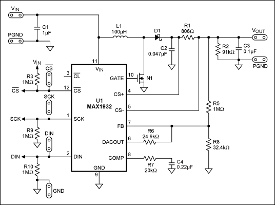
If we go to the datasheet for the MAX1932 figure 1 page 10, we can see that the "comp" (compensation) pin, is connected to the Verror signal. So this signal is "integrated" (or at least "stabilized") before being fed into the ramp comparator. This is typical of how switching converters work. (There are some chips that do not provide a pin for external control of compensation.)

My question is: How is this control loop supposed to keep the output voltage steady regardless of for instance, load variations, if the error being reduced to zero would actually stop the switching?

In the absence of compensation, a given error signal will cause a given duty cycle to be generated. If the given error signal is "zero", some particular duty cycle will be generated. That duty cycle will not be zero, nor 100%, but somewhere in the middle. If the error signal goes positive or negative, the duty cycle will become greater or smaller appropriately.

Let's call the duty cycle generated by a zero error signal \$D_0\$.

Let's call the output voltage for which the converter is designed \$V_0\$

If a duty cycle of \$D_0\$ causes the converter to output \$V_0\$, then the error signal generated by the output will also be zero. The converter can possibly be stable at this point.

If a duty cycle of \$D_0\$ causes the converter to output a voltage different from \$V_0\$, then the circuit will not be stable at its designed output voltage. There might be a stable point very near the designed output voltage. Alternatively, the output voltage may oscillate around some point near the designed output voltage. The compensation referred to previously is intended to stabilize the circuit, and prevent such oscillations.

A comparison I have used to understand it better is when I think of a PI controller, which brings the error to zero but has a memory in its output value, so it only responds to small variations once the steady state value is reached.

That is indeed how the control circuit of a switching converter generally works. The diagram in your question does not accurately show this. However, the next diagram in the tutorial helps a little.

enter image description here

Pin 8, in that diagram is connected to a resistor, capacitor pair, and these provide the "integral" part of the control.

If we go to the datasheet for the MAX1932 figure 1 page 10, we can see that the "comp" (compensation) pin, is connected to the Verror signal. So this signal is "integrated" (or at least "stabilized") before being fed into the ramp comparator.

A comparison I have used to understand it better is when I think of a PI controller, which brings the error to zero but has a memory in its output value, so it only responds to small variations once the steady state value is reached.

That is indeed how the control circuit of a switching converter generally works. The diagram in your question does not accurately show this. However, the next diagram in the tutorial helps a little.

enter image description here

Pin 8, in that diagram is connected to a resistor, capacitor pair, and these provide the "integral" part of the control.

If we go to the datasheet for the MAX1932 figure 1 page 10, we can see that the "comp" (compensation) pin, is connected to the Verror signal. So this signal is "integrated" (or at least "stabilized") before being fed into the ramp comparator. This is typical of how switching converters work. (There are some chips that do not provide a pin for external control of compensation.)

My question is: How is this control loop supposed to keep the output voltage steady regardless of for instance, load variations, if the error being reduced to zero would actually stop the switching?

In the absence of compensation, a given error signal will cause a given duty cycle to be generated. If the given error signal is "zero", some particular duty cycle will be generated. That duty cycle will not be zero, nor 100%, but somewhere in the middle. If the error signal goes positive or negative, the duty cycle will become greater or smaller appropriately.

Let's call the duty cycle generated by a zero error signal \$D_0\$.

Let's call the output voltage for which the converter is designed \$V_0\$

If a duty cycle of \$D_0\$ causes the converter to output \$V_0\$, then the error signal generated by the output will also be zero. The converter can possibly be stable at this point.

If a duty cycle of \$D_0\$ causes the converter to output a voltage different from \$V_0\$, then the circuit will not be stable at its designed output voltage. There might be a stable point very near the designed output voltage. Alternatively, the output voltage may oscillate around some point near the designed output voltage. The compensation referred to previously is intended to stabilize the circuit, and prevent such oscillations.

added 29 characters in body
Source Link
Math Keeps Me Busy
  • 27.9k
  • 5
  • 25
  • 87

A comparison I have used to understand it better is when I think of a PI controller, which brings the error to zero but has a memory in its output value, so it only responds to small variations once the steady state value is reached.

That is indeed how the control circuit of a switching converter generally works. The diagram in your question does not accurately show this. However, the next diagram in the tutorial helps a little.

enter image description here

Pin 8, in that diagram is connected to a resistor, capacitor pair, and these provide the "integral" part of the control.

If we go to the datasheet for the MAX1932 figure 1 page 10, we can see that the "comp" (compensation) pin, is connected to the Verror signal. So this signal is integrated"integrated" (or at least "stabilized") before being fed into the ramp comparator.

A comparison I have used to understand it better is when I think of a PI controller, which brings the error to zero but has a memory in its output value, so it only responds to small variations once the steady state value is reached.

That is indeed how the control circuit of a switching converter generally works. The diagram in your question does not accurately show this. However, the next diagram in the tutorial helps a little.

enter image description here

Pin 8, in that diagram is connected to a resistor, capacitor pair, and these provide the "integral" part of the control.

If we go to the datasheet for the MAX1932 figure 1 page 10, we can see that the "comp" (compensation) pin, is connected to the Verror signal. So this signal is integrated before being fed into the ramp comparator.

A comparison I have used to understand it better is when I think of a PI controller, which brings the error to zero but has a memory in its output value, so it only responds to small variations once the steady state value is reached.

That is indeed how the control circuit of a switching converter generally works. The diagram in your question does not accurately show this. However, the next diagram in the tutorial helps a little.

enter image description here

Pin 8, in that diagram is connected to a resistor, capacitor pair, and these provide the "integral" part of the control.

If we go to the datasheet for the MAX1932 figure 1 page 10, we can see that the "comp" (compensation) pin, is connected to the Verror signal. So this signal is "integrated" (or at least "stabilized") before being fed into the ramp comparator.

Source Link
Math Keeps Me Busy
  • 27.9k
  • 5
  • 25
  • 87

A comparison I have used to understand it better is when I think of a PI controller, which brings the error to zero but has a memory in its output value, so it only responds to small variations once the steady state value is reached.

That is indeed how the control circuit of a switching converter generally works. The diagram in your question does not accurately show this. However, the next diagram in the tutorial helps a little.

enter image description here

Pin 8, in that diagram is connected to a resistor, capacitor pair, and these provide the "integral" part of the control.

If we go to the datasheet for the MAX1932 figure 1 page 10, we can see that the "comp" (compensation) pin, is connected to the Verror signal. So this signal is integrated before being fed into the ramp comparator.