how How to read and understand the connections  / tracestraces in a schematic?

I'mI am in the process of rebuilding a dell laptop XX327 battery pack. (xx327). I'veI have removed the outer plastic from the 18650 3s2p3S2P battery pack. I plan on replacing all six cells, reprogramming the smart battery board after spot welding new cells to the board to reset the total mah,mAh and cycle counter for the board.

I came across a great youtube video where the author does exactly what I'mI am attempting todoto do. heHe ends up building two distinct adapters to interface with the contact pins on the battery pack. I have begun to assemble the adapter to interface with my battery pack, however, I don't understand his schematic, and I'm, I am not the best at reading and understanding schematics in general.

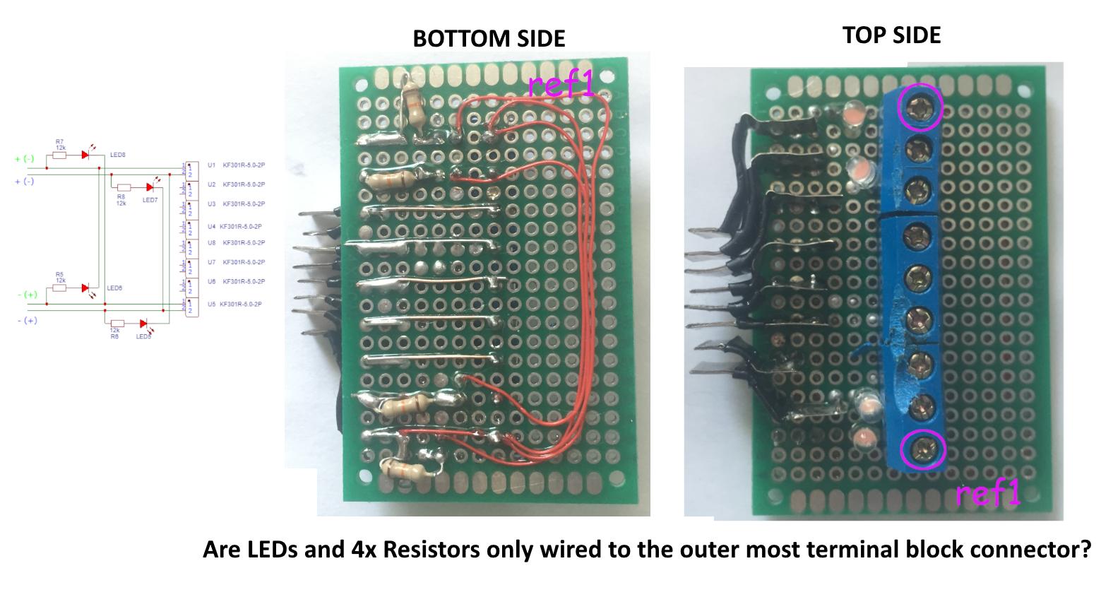
He shares a link of He shares two different schematics (shown below) for the adapter boards, one is large and one is small. I've begun to assemble/solder the larger of the two boards I've begun to assemble/solder the larger of the two boards.(also shown below).

However, i'mI am confused inabout how he wires up the resistors and diodes to the outermost terminal blocks on the prototype board. inIn the smallersmall schematic of the two examples, it looks like 4 LEDs are wired to the 4 outermost contact points/terminal blocks, whereas the larger of whereas on the schematicslarge schematic it looks he is only wiringlike the ledsLEDs are wired to the 2 outermost terminal blocks, thus my confusion and my posting of this question.

iI hope somebody can help with my understanding ofme understand the wiring of this adapter board.

  Also, if there is something i'mI am leaving out, please let me know, and i'llI will update my question.

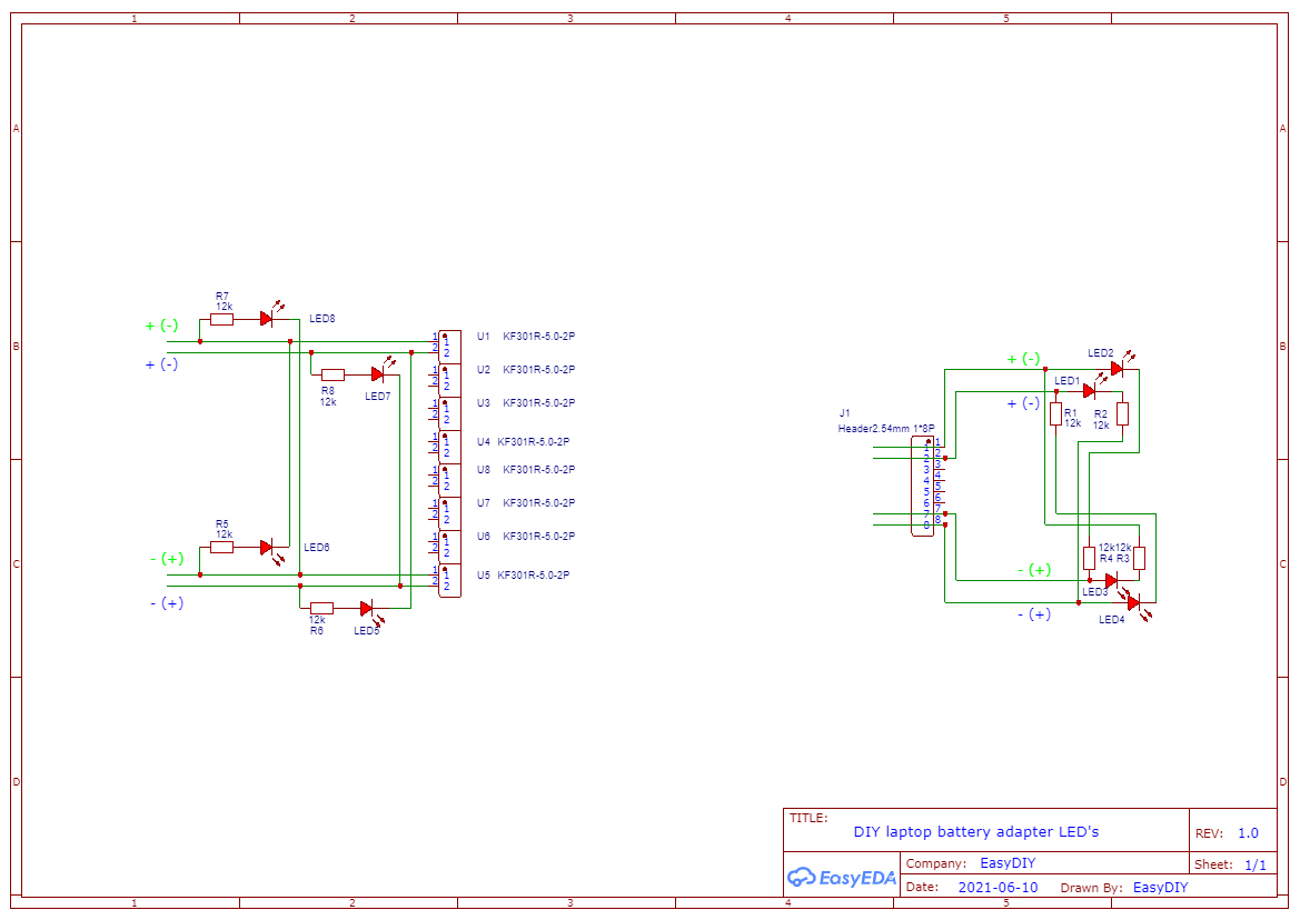
The Schematic

enter image description here

Soldered Board

enter image description here

how to read understand the connections  / traces in a schematic

I'm in the process of rebuilding a dell laptop battery pack. (xx327). I've removed the outer plastic from the 18650 3s2p battery pack. I plan on replacing all six cells, reprogramming the smart battery board after spot welding new cells to the board to reset the total mah, and cycle counter for the board.

I came across a great youtube video where the author does exactly what I'm attempting todo. he ends up building two distinct adapters to interface with the contact pins on the battery pack. I have begun to assemble the adapter to interface with my battery pack, however I don't understand his schematic, and I'm not the best at reading and understanding schematics in general.

He shares a link of two different schematics for the adapter boards, one is large and one is small. I've begun to assemble/solder the larger of the two boards.

However, i'm confused in how he wires up the resistors and diodes to the outermost terminal blocks on the prototype board. in the smaller schematic of the two examples it looks like 4 LEDs are wired to the 4 outermost contact points/terminal blocks, whereas the larger of the schematics it looks he is only wiring the leds to the 2 outermost terminal blocks, thus my confusion and my posting of this question.

i hope somebody can help with my understanding of the wiring of this adapter board.

  if there is something i'm leaving out, please let me know, and i'll update my question.

How to read and understand the connections/traces in a schematic?

I am in the process of rebuilding a dell laptop XX327 battery pack. I have removed the outer plastic from the 18650 3S2P battery pack. I plan on replacing all six cells, reprogramming the smart battery board after spot welding new cells to the board to reset the total mAh and cycle counter for the board.

I came across a great youtube video where the author does exactly what I am attempting to do. He ends up building two distinct adapters to interface with the contact pins on the battery pack. I have begun to assemble the adapter to interface with my battery pack, however, I don't understand his schematic and, I am not the best at reading and understanding schematics in general.

He shares two different schematics (shown below) for the adapter boards, one is large and one is small. I've begun to assemble/solder the larger of the two boards (also shown below).

However, I am confused about how he wires up the resistors and diodes to the outermost terminal blocks on the prototype board. In the small schematic, it looks like 4 LEDs are wired to the 4 outermost contact points/terminal blocks whereas on the large schematic it looks like the LEDs are wired to the 2 outermost terminal blocks, thus my confusion and my posting of this question.

I hope somebody can help me understand the wiring of this adapter board. Also, if there is something I am leaving out, please let me know and I will update my question.

The Schematic

enter image description here

Soldered Board

enter image description here

Source Link
ipatch
  • 201
  • 1
  • 8

how to read understand the connections / traces in a schematic

I'm in the process of rebuilding a dell laptop battery pack. (xx327). I've removed the outer plastic from the 18650 3s2p battery pack. I plan on replacing all six cells, reprogramming the smart battery board after spot welding new cells to the board to reset the total mah, and cycle counter for the board.

I came across a great youtube video where the author does exactly what I'm attempting todo. he ends up building two distinct adapters to interface with the contact pins on the battery pack. I have begun to assemble the adapter to interface with my battery pack, however I don't understand his schematic, and I'm not the best at reading and understanding schematics in general.

He shares a link of two different schematics for the adapter boards, one is large and one is small. I've begun to assemble/solder the larger of the two boards.

However, i'm confused in how he wires up the resistors and diodes to the outermost terminal blocks on the prototype board. in the smaller schematic of the two examples it looks like 4 LEDs are wired to the 4 outermost contact points/terminal blocks, whereas the larger of the schematics it looks he is only wiring the leds to the 2 outermost terminal blocks, thus my confusion and my posting of this question.

i hope somebody can help with my understanding of the wiring of this adapter board.

if there is something i'm leaving out, please let me know, and i'll update my question.