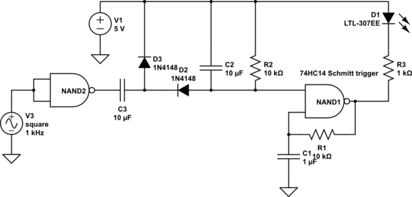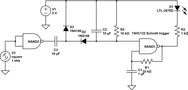

simulate this circuitsimulate this circuit – Schematic created using CircuitLab
I haven't tested this, but it looks similar to what you want. R1 and C1 set the output blink frequency when the input is constant (either hi or lo). R2 and C2 set the delay time from when the input stops pulsing to when the output starts blinking. When the input is constant, R2 eventually drains C2 and enables the oscillator to blink. When the input oscillates, C2 and the diodes charge up C2, so that NAND1 input goes close to GND, and then the output of NAND1 stays hi, and then D1 stays dark.
