deleted 2 characters in body
Source Link
JRE
  • 73.5k
  • 10
  • 112
  • 194

I am trying to design a simple battery operated circuit (ESP8266) controlled by a MOSFET (schematic below).

enter image description here

I was going through certainsome videos to understand better and came across this video: https://www.youtubethis video.com/watch?v=XVoAI86Wo7o.

He talks about about the MOSFET VDS requirement to be 0.5 V at 2.57 time. He is subtracting the min voltage requirement of ESP8266 which is 2.5 V from a battery voltage of 3.0 V and thereby determining the VDS to be 0.5 V.

I thought the VDS is the max voltage that can flow between the source and drain terminals which in this case is 4.2 V. What am I missing? Are the following calculations correct? I seem to be confused with this.

The P-channel controls the high side positive rail to MCU while the N-channel controls the P-channel MOSFET.

VDS(max) across PFET will be maximum 4.2 V and min of 3 V when used with a LIPO.

VGS(min) across PFET = -3 V

VDS(max) across NFET will also be 4.2 V

VGS(min) across NFET = 3 V

IDD continuous across PFET will be a max of 300 mA

I am trying to design a simple battery operated circuit (ESP8266) controlled by a MOSFET (schematic below).

enter image description here

I was going through certain videos to understand better and came across this video: https://www.youtube.com/watch?v=XVoAI86Wo7o.

He talks about about the MOSFET VDS requirement to be 0.5 V at 2.57 time. He is subtracting the min voltage requirement of ESP8266 which is 2.5 V from a battery voltage of 3.0 V and thereby determining the VDS to be 0.5 V.

I thought the VDS is the max voltage that can flow between the source and drain terminals which in this case is 4.2 V. What am I missing? Are the following calculations correct? I seem to be confused with this.

The P-channel controls the high side positive rail to MCU while the N-channel controls the P-channel MOSFET.

VDS(max) across PFET will be maximum 4.2 V and min of 3 V when used with a LIPO.

VGS(min) across PFET = -3 V

VDS(max) across NFET will also be 4.2 V

VGS(min) across NFET = 3 V

IDD continuous across PFET will be a max of 300 mA
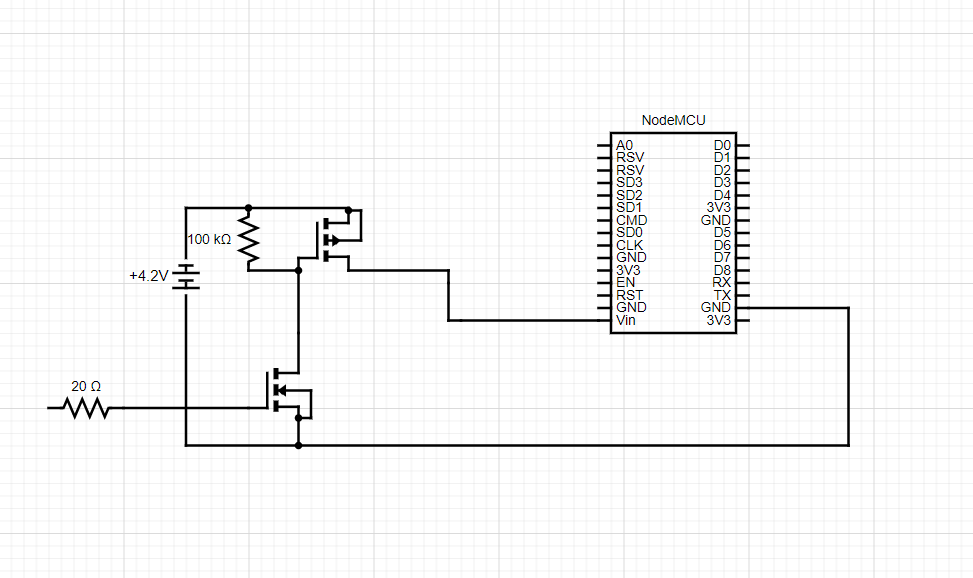
I am trying to design a simple battery operated circuit (ESP8266) controlled by a MOSFET (schematic below).

enter image description here

I was going through some videos to understand better and came across this video.

He talks about about the MOSFET VDS requirement to be 0.5 V at 2.57 time. He is subtracting the min voltage requirement of ESP8266 which is 2.5 V from a battery voltage of 3.0 V and thereby determining the VDS to be 0.5 V.

I thought the VDS is the max voltage that can flow between the source and drain terminals which in this case is 4.2 V. What am I missing? Are the following calculations correct? I seem to be confused with this.

The P-channel controls the high side positive rail to MCU while the N-channel controls the P-channel MOSFET.

VDS(max) across PFET will be maximum 4.2 V and min of 3 V when used with a LIPO.

VGS(min) across PFET = -3 V

VDS(max) across NFET will also be 4.2 V

VGS(min) across NFET = 3 V

IDD continuous across PFET will be a max of 300 mA

added 194 characters in body; edited title
Source Link
Velvet
  • 4.7k
  • 5
  • 18
  • 32

Mosfet as Design confusion with a MOSFET as switch design confusion

enter image description hereI I am trying to design a simple battery operated circuit (ESP8266) controlled by a MosfetMOSFET (schematic attachedbelow).

enter image description here

I was going through certain videos to understand better and came across this video  : https://www.youtube.com/watch?v=XVoAI86Wo7o.

He talks about about the mosfet VdsMOSFET VDS requirement to be 0.5V5 V at 2.57 time. He is subtracting the min voltage requirement of ESP8266 which is 2.5V5 V from a battery voltage of 3.0 V and thereby determining the VdsVDS to be 0.5 V.

I thought the VdsVDS is the max voltage that can be flow between the source and drain terminals which in this case is 4.2V2 V. What am iI missing.? Are the following calculations correct.? I seem to be confused with this.

The P Channel-channel controls the high side positive rail to MCU while the N Channel-channel controls the P Channel Mosfet-channel MOSFET.

Vds maxVDS(max) across PFET will be maximum 4.2V2 V and min of 3 V when used with a LIPO.

min VgsVGS(min) across PFET = -3 V

Vds maxVDS(max) across NFET will also be 4.2V2 V

min VgsVGS(min) across NFET = 3 V

Idd continousIDD continuous across PFET will be a max of 300mA300 mA

Mosfet as a switch design confusion

enter image description hereI am trying to design a simple battery operated circuit (ESP8266) controlled by a Mosfet (schematic attached). I was going through certain videos to understand better and came across this video  https://www.youtube.com/watch?v=XVoAI86Wo7o.

He talks about about the mosfet Vds requirement to be 0.5V at 2.57 time. He is subtracting the min voltage requirement of ESP8266 which is 2.5V from a battery voltage of 3.0 and thereby determining the Vds to be 0.5.

I thought the Vds is the max voltage that can be flow between the source and drain terminals which in this case is 4.2V. What am i missing. Are the following calculations correct. I seem to be confused with this.

The P Channel controls the high side positive rail to MCU while the N Channel controls the P Channel Mosfet.

Vds max across PFET will be maximum 4.2V and min of 3 when used with a LIPO.

min Vgs across PFET = -3

Vds max across NFET will also be 4.2V

min Vgs across NFET = 3

Idd continous across PFET will be a max of 300mA

Design confusion with a MOSFET as switch

I am trying to design a simple battery operated circuit (ESP8266) controlled by a MOSFET (schematic below).

enter image description here

I was going through certain videos to understand better and came across this video: https://www.youtube.com/watch?v=XVoAI86Wo7o.

He talks about about the MOSFET VDS requirement to be 0.5 V at 2.57 time. He is subtracting the min voltage requirement of ESP8266 which is 2.5 V from a battery voltage of 3.0 V and thereby determining the VDS to be 0.5 V.

I thought the VDS is the max voltage that can flow between the source and drain terminals which in this case is 4.2 V. What am I missing? Are the following calculations correct? I seem to be confused with this.

The P-channel controls the high side positive rail to MCU while the N-channel controls the P-channel MOSFET.

VDS(max) across PFET will be maximum 4.2 V and min of 3 V when used with a LIPO.

VGS(min) across PFET = -3 V

VDS(max) across NFET will also be 4.2 V

VGS(min) across NFET = 3 V

IDD continuous across PFET will be a max of 300 mA

Source Link
Suresh Kumar
  • 193
  • 1
  • 3
  • 15

Mosfet as a switch design confusion

enter image description hereI am trying to design a simple battery operated circuit (ESP8266) controlled by a Mosfet (schematic attached). I was going through certain videos to understand better and came across this video https://www.youtube.com/watch?v=XVoAI86Wo7o.

He talks about about the mosfet Vds requirement to be 0.5V at 2.57 time. He is subtracting the min voltage requirement of ESP8266 which is 2.5V from a battery voltage of 3.0 and thereby determining the Vds to be 0.5.

I thought the Vds is the max voltage that can be flow between the source and drain terminals which in this case is 4.2V. What am i missing. Are the following calculations correct. I seem to be confused with this.

The P Channel controls the high side positive rail to MCU while the N Channel controls the P Channel Mosfet.

Vds max across PFET will be maximum 4.2V and min of 3 when used with a LIPO.

min Vgs across PFET = -3

Vds max across NFET will also be 4.2V

min Vgs across NFET = 3

Idd continous across PFET will be a max of 300mA