deleted 118 characters in body
Source Link

The problem is, I connected the battery's negative terminal to VIN- and the PCB is already assembled and everything.

The PCB will have to change, since connecting any high-power source directly to the A/D inputs is ill advised. You need some sort of overcurrent protection should the ADC fail, or should there be transients on the battery that will kill the ADC, turn it into a resistor, and proceed to destroy the MCU.

It is fine to start prototypes with a PCB layout, as - if you're quick at it, and have many products in the pipeline - it will speed things up vs. sticking wires into holes on a breadboard. But that doesn't mean you should expect that PCB to survive unchanged after you began to test it - especially if you don't have much experience with such circuits and can't be quite sure based on past projects that there's a good chance it will work as-is.

So, it's all right as long as you treat the PCB as the prototype it is - and expect, as you should, that there will be a 2nd PCB in the works after you correct mistakes.

The connection of battery's (-) terminal to GND is OK for basic functionality. But: ADS1110's single-ended input range is 0-2.048V. So, you'd be wasting one bit of resolution by connecting the battery directly to the ADC.

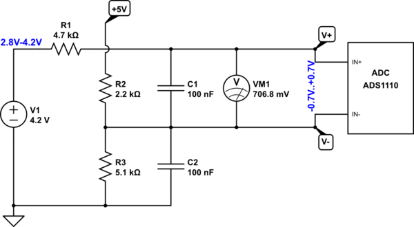
We need to map the 0-5V voltage to the differential input range of the ADC. Ideally, 0V should be about -2V, and 5V should be about +2V differential.

Using a 5V ADC supply, we can have the following circuit:
schematic

simulate this circuit – Schematic created using CircuitLab

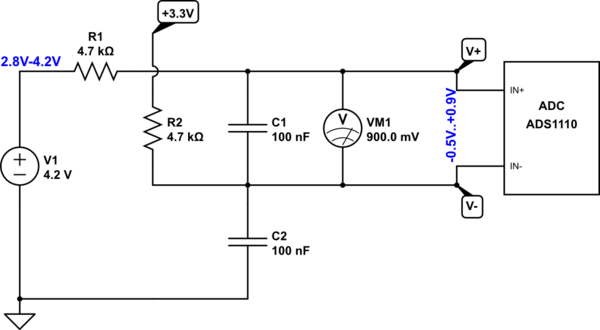
It doesn't use the full ADC input range, since there's no amplification available, but it does the job. Similarly, we can make it work for a 3.3V VCC:
schematic

simulate this circuit

An alternative approach could offset the input voltage - the resolution is the same as above, but the stability of the 3.3V supply is not influencing the measurement anymore. A lower current reference such as LM385-2.5 etc. should be used to lower the quiescent current. There are excellent, modern, micropower references that could be used for that purpose.

schematic

simulate this circuit

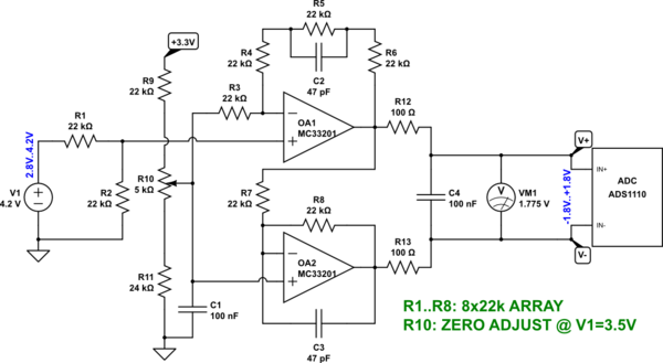
Alternatively, we could use a double op-amp to convert the single-ended battery input to a fully differential voltage:
schematic

simulate this circuit

The zero adjustment should be set at battery voltage of 3.5V: the ADC input voltage should be 0V differential (between V+ and V-).

Using a thick-film or thin-film array for R1..R8 improves the stability of the circuit, as well as minimizing the unadjusted error, since the resistor ratios in an array typically match better than their absolute values, even if the array's ratio tolerance is not specified.

OA1, OA2 are two halves of just about any low power rail-to-rail input/output (RRIO) op-amp. It could be a micropower or nanopower type with 40-50kHZ GBW, or higher.

The problem is, I connected the battery's negative terminal to VIN- and the PCB is already assembled and everything.

The PCB will have to change, since connecting any high-power source directly to the A/D inputs is ill advised. You need some sort of overcurrent protection should the ADC fail, or should there be transients on the battery that will kill the ADC, turn it into a resistor, and proceed to destroy the MCU.

It is fine to start prototypes with a PCB layout, as - if you're quick at it, and have many products in the pipeline - it will speed things up vs. sticking wires into holes on a breadboard. But that doesn't mean you should expect that PCB to survive unchanged after you began to test it - especially if you don't have much experience with such circuits and can't be quite sure based on past projects that there's a good chance it will work as-is.

So, it's all right as long as you treat the PCB as the prototype it is - and expect, as you should, that there will be a 2nd PCB in the works after you correct mistakes.

The connection of battery's (-) terminal to GND is OK for basic functionality. But: ADS1110's single-ended input range is 0-2.048V. So, you'd be wasting one bit of resolution by connecting the battery directly to the ADC.

We need to map the 0-5V voltage to the differential input range of the ADC. Ideally, 0V should be about -2V, and 5V should be about +2V differential.

Using a 5V ADC supply, we can have the following circuit:

schematic

simulate this circuit – Schematic created using CircuitLab

It doesn't use the full ADC input range, since there's no amplification available, but it does the job. Similarly, we can make it work for a 3.3V VCC:

schematic

simulate this circuit

An alternative approach could offset the input voltage - the resolution is the same as above, but the stability of the 3.3V supply is not influencing the measurement anymore. A lower current reference such as LM385-2.5 etc. should be used to lower the quiescent current. There are excellent, modern, micropower references that could be used for that purpose.

schematic

simulate this circuit

Alternatively, we could use a double op-amp to convert the single-ended battery input to a fully differential voltage:

schematic

simulate this circuit

The zero adjustment should be set at battery voltage of 3.5V: the ADC input voltage should be 0V differential (between V+ and V-).

Using a thick-film or thin-film array for R1..R8 improves the stability of the circuit, as well as minimizing the unadjusted error, since the resistor ratios in an array typically match better than their absolute values, even if the array's ratio tolerance is not specified.

OA1, OA2 are two halves of just about any low power rail-to-rail input/output (RRIO) op-amp. It could be a micropower or nanopower type with 40-50kHZ GBW, or higher.

deleted 118 characters in body
Source Link

The problem is, I connected the battery's negative terminal to VIN- and the PCB is already assembled and everything.

The PCB will have to change, since connecting any high-power source directly to the A/D inputs is ill advised. You need some sort of overcurrent protection should the ADC fail, or should there be transients on the battery that will kill the ADC, turn it into a resistor, and proceed to destroy the MCU.

It is fine to start prototypes with a PCB layout, as - if you're quick at it, and have many products in the pipeline - it will speed things up vs. sticking wires into holes on a breadboard. But that doesn't mean you should expect that PCB to survive unchanged after you began to test it - especially if you don't have much experience with such circuits and can't be quite sure based on past projects that there's a good chance it will work as-is.

So, it's all right as long as you treat the PCB as the prototype it is - and expect, as you should, that there will be a 2nd PCB in the works after you correct mistakes.

The connection of battery's (-) terminal to GND is OK for basic functionality. But: ADS1110's single-ended input range is 0-2.048V. So, you'd be wasting one bit of resolution by connecting the battery directly to the ADC.

We need to map the 0-5V voltage to the differential input range of the ADC. Ideally, 0V should be about -2V, and 5V should be about +2V differential.

Using a 5V ADC supply, we can have the following circuit:

schematicschematic

simulate this circuitsimulate this circuit – Schematic created using CircuitLab

It doesn't use the full ADC input range, since there's no amplification available, but it does the job. Similarly, we can make it work for a 3.3V VCC:

schematicschematic

simulate this circuitsimulate this circuit

To useAn alternative approach could offset the full input range ofvoltage - the ADCresolution is the same as above, we'd need simplified single-ended-to-differential conversion using an opbut the stability of the 3.3V supply is not influencing the measurement anymore. A lower current reference such as LM385-amp2.5 etc. should be used to lower the quiescent current. There are excellent, modern, micropower references that could be used for that purpose.

schematic http://--i.stack.imgur.com/w0Ffk.pngschematic

simulate this circuitsimulate this circuit

The problem is, I connected the battery's negative terminal to VIN- and the PCB is already assembled and everything.

The PCB will have to change, since connecting any high-power source directly to the A/D inputs is ill advised. You need some sort of overcurrent protection should the ADC fail, or should there be transients on the battery that will kill the ADC, turn it into a resistor, and proceed to destroy the MCU.

It is fine to start prototypes with a PCB layout, as - if you're quick at it, and have many products in the pipeline - it will speed things up vs. sticking wires into holes on a breadboard. But that doesn't mean you should expect that PCB to survive unchanged after you began to test it - especially if you don't have much experience with such circuits and can't be quite sure based on past projects that there's a good chance it will work as-is.

So, it's all right as long as you treat the PCB as the prototype it is - and expect, as you should, that there will be a 2nd PCB in the works after you correct mistakes.

The connection of battery's (-) terminal to GND is OK for basic functionality. But: ADS1110's single-ended input range is 0-2.048V. So, you'd be wasting one bit of resolution by connecting the battery directly to the ADC.

We need to map the 0-5V voltage to the differential input range of the ADC. Ideally, 0V should be about -2V, and 5V should be about +2V differential.

Using a 5V ADC supply, we can have the following circuit:

schematic

simulate this circuit – Schematic created using CircuitLab

It doesn't use the full ADC input range, since there's no amplification available, but it does the job. Similarly, we can make it work for a 3.3V VCC:

schematic

simulate this circuit

To use the full input range of the ADC, we'd need simplified single-ended-to-differential conversion using an op-amp.

schematic http://--i.stack.imgur.com/w0Ffk.png

simulate this circuit

The problem is, I connected the battery's negative terminal to VIN- and the PCB is already assembled and everything.

The PCB will have to change, since connecting any high-power source directly to the A/D inputs is ill advised. You need some sort of overcurrent protection should the ADC fail, or should there be transients on the battery that will kill the ADC, turn it into a resistor, and proceed to destroy the MCU.

It is fine to start prototypes with a PCB layout, as - if you're quick at it, and have many products in the pipeline - it will speed things up vs. sticking wires into holes on a breadboard. But that doesn't mean you should expect that PCB to survive unchanged after you began to test it - especially if you don't have much experience with such circuits and can't be quite sure based on past projects that there's a good chance it will work as-is.

So, it's all right as long as you treat the PCB as the prototype it is - and expect, as you should, that there will be a 2nd PCB in the works after you correct mistakes.

The connection of battery's (-) terminal to GND is OK for basic functionality. But: ADS1110's single-ended input range is 0-2.048V. So, you'd be wasting one bit of resolution by connecting the battery directly to the ADC.

We need to map the 0-5V voltage to the differential input range of the ADC. Ideally, 0V should be about -2V, and 5V should be about +2V differential.

Using a 5V ADC supply, we can have the following circuit:

schematic

simulate this circuit – Schematic created using CircuitLab

It doesn't use the full ADC input range, since there's no amplification available, but it does the job. Similarly, we can make it work for a 3.3V VCC:

schematic

simulate this circuit

An alternative approach could offset the input voltage - the resolution is the same as above, but the stability of the 3.3V supply is not influencing the measurement anymore. A lower current reference such as LM385-2.5 etc. should be used to lower the quiescent current. There are excellent, modern, micropower references that could be used for that purpose.

schematic

simulate this circuit

deleted 118 characters in body
Source Link

The problem is, I connected the battery's negative terminal to VIN- and the PCB is already assembled and everything.

The PCB will have to change, since connecting any high-power source directly to the A/D inputs is ill advised. You need some sort of overcurrent protection should the ADC fail, or should there be transients on the battery that will kill the ADC, turn it into a resistor, and proceed to destroy the MCU.

It is fine to start prototypes with a PCB layout, as - if you're quick at it, and have many products in the pipeline - it will speed things up vs. sticking wires into holes on a breadboard. But that doesn't mean you should expect that PCB to survive unchanged after you began to test it - especially if you don't have much experience with such circuits and can't be quite sure based on past projects that there's a good chance it will work as-is.

So, it's all right as long as you treat the PCB as the prototype it is - and expect, as you should, that there will be a 2nd PCB in the works after you correct mistakes.

The connection of battery's (-) terminal to GND is OK for basic functionality. But: ADS1110's single-ended input range is 0-2.048V. So, you'd be wasting one bit of resolution by connecting the battery directly to the ADC.

We need to map the 0-5V voltage to the differential input range of the ADC. Ideally, 0V should be about -2V, and 5V should be about +2V differential.

If you hadUsing a stable 5V ADC supply as a reference, this circuit would towe can have the trickfollowing circuit:

schematicschematic

simulate this circuitsimulate this circuit – Schematic created using CircuitLab

But that's not always feasible, and an even better circuit wouldIt doesn't use a slightly lower impedance reference to generate the V- input for the full ADC:

schematic

simulate this circuit

The ubiquitous TL491 generates input range, since there's no amplification available, but it does the 2.5Vjob.

For Similarly, we can make it work for a 3.3V supply voltage, the simplest circuit wastes one bit of resolution, but doesn't require active componentsVCC:

schematicschematic

simulate this circuitsimulate this circuit

To getuse the full differential voltage swing would requireinput range of the ADC, we'd need simplified single-ended-to-differential conversion using an op-amp.

schematic http://--i.stack.imgur.com/w0Ffk.png

simulate this circuit

The problem is, I connected the battery's negative terminal to VIN- and the PCB is already assembled and everything.

The PCB will have to change, since connecting any high-power source directly to the A/D inputs is ill advised. You need some sort of overcurrent protection should the ADC fail, or should there be transients on the battery that will kill the ADC, turn it into a resistor, and proceed to destroy the MCU.

It is fine to start prototypes with a PCB layout, as - if you're quick at it, and have many products in the pipeline - it will speed things up vs. sticking wires into holes on a breadboard. But that doesn't mean you should expect that PCB to survive unchanged after you began to test it - especially if you don't have much experience with such circuits and can't be quite sure based on past projects that there's a good chance it will work as-is.

So, it's all right as long as you treat the PCB as the prototype it is - and expect, as you should, that there will be a 2nd PCB in the works after you correct mistakes.

The connection of battery's (-) terminal to GND is OK for basic functionality. But: ADS1110's single-ended input range is 0-2.048V. So, you'd be wasting one bit of resolution by connecting the battery directly to the ADC.

We need to map the 0-5V voltage to the differential input range of the ADC. Ideally, 0V should be about -2V, and 5V should be about +2V differential.

If you had a stable 5V supply as a reference, this circuit would to the trick:

schematic

simulate this circuit – Schematic created using CircuitLab

But that's not always feasible, and an even better circuit would use a slightly lower impedance reference to generate the V- input for the ADC:

schematic

simulate this circuit

The ubiquitous TL491 generates the 2.5V.

For 3.3V supply voltage, the simplest circuit wastes one bit of resolution, but doesn't require active components:

schematic

simulate this circuit

To get full differential voltage swing would require an op-amp.

The problem is, I connected the battery's negative terminal to VIN- and the PCB is already assembled and everything.

The PCB will have to change, since connecting any high-power source directly to the A/D inputs is ill advised. You need some sort of overcurrent protection should the ADC fail, or should there be transients on the battery that will kill the ADC, turn it into a resistor, and proceed to destroy the MCU.

It is fine to start prototypes with a PCB layout, as - if you're quick at it, and have many products in the pipeline - it will speed things up vs. sticking wires into holes on a breadboard. But that doesn't mean you should expect that PCB to survive unchanged after you began to test it - especially if you don't have much experience with such circuits and can't be quite sure based on past projects that there's a good chance it will work as-is.

So, it's all right as long as you treat the PCB as the prototype it is - and expect, as you should, that there will be a 2nd PCB in the works after you correct mistakes.

The connection of battery's (-) terminal to GND is OK for basic functionality. But: ADS1110's single-ended input range is 0-2.048V. So, you'd be wasting one bit of resolution by connecting the battery directly to the ADC.

We need to map the 0-5V voltage to the differential input range of the ADC. Ideally, 0V should be about -2V, and 5V should be about +2V differential.

Using a 5V ADC supply, we can have the following circuit:

schematic

simulate this circuit – Schematic created using CircuitLab

It doesn't use the full ADC input range, since there's no amplification available, but it does the job. Similarly, we can make it work for a 3.3V VCC:

schematic

simulate this circuit

To use the full input range of the ADC, we'd need simplified single-ended-to-differential conversion using an op-amp.

schematic http://--i.stack.imgur.com/w0Ffk.png

simulate this circuit

Source Link
Loading