Added ground information to circuit diagram
Source Link
user319836
  • 17.1k
  • 3
  • 12
  • 43

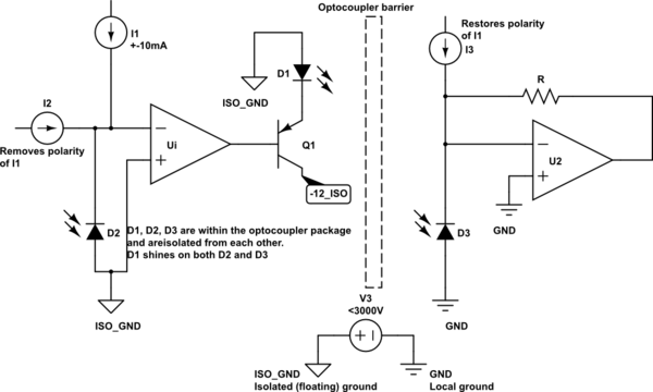
A simplified circuit diagram is shown below.

The designer used four optocouplers to obtain a current range more suitable for the feedback diode.

The optocoupler photodiodes used for feedback are all in parallel and so are represented by a single photodiode D2 with 4 times the current capability.

The photodiodes on the other side of the barrier are also in parallel so are represented by a single photodiode D3 with 4 times the current capability.

The emitting diodes are connected in series so to keep the current through each emitter identical and so the transistor need not supply 4 times the current. The are represented by D1.

The circuitry in the small red circle is represented by the current source I2, The input voltage and the 100k resistor are represented by I1. and finally the circuitry in the large red circle is represented by I3.

But at best the current sourced by the voltage reference is 5/38300<<10 mA. So how does this work ?

The missing current is supplied by the feedback diode. I2 is chosen so that when the input current is -10mA, the current through D2 is zero. (Maybe a little higher). The photocurrent is directed from cathode to anode, so pulls current from the input node,

If I1 = -I2, then opamp feedback action will force the photodiode, I_D2, current to zero. Since the diode D2 current comes from the light falling on D2, then the light falling on D3 will be the same by design of the optocoupler.

When I1 is properly selected, the current through the emitter will always be positive. The midpoint current represents 0 volts on the HV input.

So then the light falling on D2 and D3 represent the -1000 to +1000 volts of the input. Thus the current generate by D3 also represents the same voltage range.

The transimpedance amplifier converts I_D3 to a voltage. The bias current I3 is chosen so that the output voltage is 0V for HV=0.

The feedback resistor is chosen for the desired output voltage based on the input range.


Am I completely mistaken in the role of the voltage references ?

No. Together with the op-amp input resistors. They provide the desired offset.

I did not do any calculations. But the component values don’t seem to work for a -1000V input.

Checking the full schematic diagram, the Vin is likely to be no more than about 10V. This would bring the current into range.

schematicschematic

simulate this circuitsimulate this circuit – Schematic created using CircuitLab

A simplified circuit diagram is shown below.

The designer used four optocouplers to obtain a current range more suitable for the feedback diode.

The optocoupler photodiodes used for feedback are all in parallel and so are represented by a single photodiode D2 with 4 times the current capability.

The photodiodes on the other side of the barrier are also in parallel so are represented by a single photodiode D3 with 4 times the current capability.

The emitting diodes are connected in series so to keep the current through each emitter identical and so the transistor need not supply 4 times the current. The are represented by D1.

The circuitry in the small red circle is represented by the current source I2, The input voltage and the 100k resistor are represented by I1. and finally the circuitry in the large red circle is represented by I3.

But at best the current sourced by the voltage reference is 5/38300<<10 mA. So how does this work ?

The missing current is supplied by the feedback diode. I2 is chosen so that when the input current is -10mA, the current through D2 is zero. (Maybe a little higher). The photocurrent is directed from cathode to anode, so pulls current from the input node,

If I1 = -I2, then opamp feedback action will force the photodiode, I_D2, current to zero. Since the diode D2 current comes from the light falling on D2, then the light falling on D3 will be the same by design of the optocoupler.

When I1 is properly selected, the current through the emitter will always be positive. The midpoint current represents 0 volts on the HV input.

So then the light falling on D2 and D3 represent the -1000 to +1000 volts of the input. Thus the current generate by D3 also represents the same voltage range.

The transimpedance amplifier converts I_D3 to a voltage. The bias current I3 is chosen so that the output voltage is 0V for HV=0.

The feedback resistor is chosen for the desired output voltage based on the input range.


Am I completely mistaken in the role of the voltage references ?

No. Together with the op-amp input resistors. They provide the desired offset.

I did not do any calculations. But the component values don’t seem to work for a -1000V input.

Checking the full schematic diagram, the Vin is likely to be no more than about 10V. This would bring the current into range.

schematic

simulate this circuit – Schematic created using CircuitLab

added 16 characters in body
Source Link
user319836
  • 17.1k
  • 3
  • 12
  • 43

A simplified circuit diagram is shown below.

The designer used four optocouplers to obtain a current range more suitable for the feedback diode.

The optocoupler photodiodes used for feedback are all in parallel and so are represented by a single photodiode D2 with 4 times the current capability.

The photodiodes on the other side of the barrier are also in parallel so are represented by a single photodiode D3 with 4 times the current capability.

The emitting diodes are connected in series so to keep the current through each emitter identical and so the transistor need not supply 4 times the current. The are represented by D1.

The circuitry in the small red circle is represented by the current source I2, The input voltage and the 100k resistor are represented by I1. and finally the circuitry in the large red circle is represented by I3.

But at best the current sourced by the voltage reference is 5/38300<<10 mA. So how does this work ?

The missing current is supplied by the feedback diode. I2 is chosen so that when the input current is -10mA, the current through D2 is zero. (Maybe a little higher). The photocurrent is directed from cathode to anode, so pulls current from the input node,

If I1 = I2-I2, then opamp feedback action will force the diodephotodiode, I_D2, current to zero. Since the diode currenD2 current comes from the light falling on D2, then the light falling on D3 will be the same by design of the opto coupleroptocoupler.

When I1 is properly selected, the current through the emitter will always be positive. The midpoint current represents 0 volts on the HV input.

So then the light falling on D2 and D3 represent the -1000 to +1000 volts of the input. Thus the current generate by D3 also represents the same voltage range.

The transimpedance amplifier converts I_D3 to a voltage. The bias current I3 is chosen so that the output voltage is 0V for HV=0.

The feedback resistor is chosen for the desired output voltage based on the input range.


Am I completely mistaken in the role of the voltage references ?

No. Together with the op-amp input resistors. They provide the desired offset.

I did not do any calculations. But the component values don’t seem to work for a -1000V input.

Checking the full schematic diagram, the Vin is likely to be no more than about 10V. This would bring the current into range.

schematic

simulate this circuit – Schematic created using CircuitLab

A simplified circuit diagram is shown below.

The designer used four optocouplers to obtain a current range more suitable for the feedback diode.

The optocoupler photodiodes used for feedback are all in parallel and so are represented by a single photodiode D2 with 4 times the current capability.

The photodiodes on the other side of the barrier are also in parallel so are represented by a single photodiode D3 with 4 times the current capability.

The emitting diodes are connected in series so to keep the current through each emitter identical and so the transistor need not supply 4 times the current. The are represented by D1.

The circuitry in the small red circle is represented by the current source I2, The input voltage and the 100k resistor are represented by I1. and finally the circuitry in the large red circle is represented by I3.

But at best the current sourced by the voltage reference is 5/38300<<10 mA. So how does this work ?

The missing current is supplied by the feedback diode. I2 is chosen so that when the input current is -10mA, the current through D2 is zero. (Maybe a little higher). The photocurrent is directed from cathode to anode, so pulls current from the input node,

If I1 = I2, then opamp feedback action will force the diode current to zero. Since the diode curren comes from the light falling on D2, then the light falling on D3 will be the same by design of the opto coupler.

When I1 is properly selected, the current through the emitter will always be positive. The midpoint current represents 0 volts on the HV input.

So then the light falling on D2 and D3 represent the -1000 to +1000 volts of the input. Thus the current generate by D3 also represents the same voltage range.

The transimpedance amplifier converts I_D3 to a voltage. The bias current I3 is chosen so that the output voltage is 0V for HV=0.

The feedback resistor is chosen for the desired output voltage based on the input range.


Am I completely mistaken in the role of the voltage references ?

No. Together with the op-amp input resistors. They provide the desired offset.

I did not do any calculations. But the component values don’t seem to work for a -1000V input.

Checking the full schematic diagram, the Vin is likely to be no more than about 10V. This would bring the current into range.

schematic

simulate this circuit – Schematic created using CircuitLab

A simplified circuit diagram is shown below.

The designer used four optocouplers to obtain a current range more suitable for the feedback diode.

The optocoupler photodiodes used for feedback are all in parallel and so are represented by a single photodiode D2 with 4 times the current capability.

The photodiodes on the other side of the barrier are also in parallel so are represented by a single photodiode D3 with 4 times the current capability.

The emitting diodes are connected in series so to keep the current through each emitter identical and so the transistor need not supply 4 times the current. The are represented by D1.

The circuitry in the small red circle is represented by the current source I2, The input voltage and the 100k resistor are represented by I1. and finally the circuitry in the large red circle is represented by I3.

But at best the current sourced by the voltage reference is 5/38300<<10 mA. So how does this work ?

The missing current is supplied by the feedback diode. I2 is chosen so that when the input current is -10mA, the current through D2 is zero. (Maybe a little higher). The photocurrent is directed from cathode to anode, so pulls current from the input node,

If I1 = -I2, then opamp feedback action will force the photodiode, I_D2, current to zero. Since the diode D2 current comes from the light falling on D2, then the light falling on D3 will be the same by design of the optocoupler.

When I1 is properly selected, the current through the emitter will always be positive. The midpoint current represents 0 volts on the HV input.

So then the light falling on D2 and D3 represent the -1000 to +1000 volts of the input. Thus the current generate by D3 also represents the same voltage range.

The transimpedance amplifier converts I_D3 to a voltage. The bias current I3 is chosen so that the output voltage is 0V for HV=0.

The feedback resistor is chosen for the desired output voltage based on the input range.


Am I completely mistaken in the role of the voltage references ?

No. Together with the op-amp input resistors. They provide the desired offset.

I did not do any calculations. But the component values don’t seem to work for a -1000V input.

Checking the full schematic diagram, the Vin is likely to be no more than about 10V. This would bring the current into range.

schematic

simulate this circuit – Schematic created using CircuitLab

added 267 characters in body
Source Link
user319836
  • 17.1k
  • 3
  • 12
  • 43

A simplified circuit diagram is shown below.

The designer used four optocouplers to obtain a current range more suitable for the feedback diode.

The optocoupler photodiodes used for feedback are all in parallel and so are represented by a single photodiode D2 with 4 times the current capability.

The photodiodes on the other side of the barrier are also in parallel so are represented by a single photodiode D3 with 4 times the current capability.

The emitting diodes are connected in series so to keep the current through each emitter identical and so the transistor need not supply 4 times the current. The are represented by D1.

The circuitry in the small red circle is represented by the current source I2, The input voltage and the 100k resistor are represented by I1. and finally the circuitry in the large red circle is represented by I3.

But at best the current sourced by the voltage reference is 5/38300<<10 mA. So how does this work ?

The missing current is supplied by the feedback diode. I2 is chosen so that when the input current is -10mA, the current through D2 is zero. (Maybe a little higher). The photocurrent is directed from cathode to anode, so pulls current from the input node,

If I1 = I2, then opamp feedback action will force the diode current to zero. Since the diode curren comes from the light falling on D2, then the light falling on D3 will be the same by design of the opto coupler.

When I1 is properly selected, the current through the emitter will always be positive. The midpoint current represents 0 volts on the HV input.

So then the light falling on D2 and D3 represent the -1000 to +1000 volts of the input. Thus the current generate by D3 also represents the same voltage range.

The transimpedance amplifier converts I_D3 to a voltage. The bias current I3 is chosen so that the output voltage is 0V for HV=0.

The feedback resistor is chosen for the desired output voltage based on the input range.


Am I completely mistaken in the role of the voltage references ?

No. Together with the op-amp input resistors. They provide the desired offset.

I did not do any calculations. But the component values don’t seem to work for a -1000V input.

Checking the full schematic diagram, the Vin is likely to be no more than about 10V. This would bring the current into range.

schematic

simulate this circuit – Schematic created using CircuitLab

A simplified circuit diagram is shown below.

The designer used four optocouplers to obtain a current range more suitable for the feedback diode.

The optocoupler photodiodes used for feedback are all in parallel and so are represented by a single photodiode D2 with 4 times the current capability.

The photodiodes on the other side of the barrier are also in parallel so are represented by a single photodiode D3 with 4 times the current capability.

The emitting diodes are connected in series so to keep the current through each emitter identical and so the transistor need not supply 4 times the current. The are represented by D1.

The circuitry in the small red circle is represented by the current source I2, The input voltage and the 100k resistor are represented by I1. and finally the circuitry in the large red circle is represented by I3.

But at best the current sourced by the voltage reference is 5/38300<<10 mA. So how does this work ?

The missing current is supplied by the feedback diode. I2 is chosen so that when the input current is -10mA, the current through D2 is zero. (Maybe a little higher). The photocurrent is directed from cathode to anode, so pulls current from the input node,

If I1 = I2, then opamp feedback action will force the diode current to zero. Since the diode curren comes from the light falling on D2, then the light falling on D3 will be the same by design of the opto coupler.

When I1 is properly selected, the current through the emitter will always be positive. The midpoint current represents 0 volts on the HV input.

So then the light falling on D2 and D3 represent the -1000 to +1000 volts of the input. Thus the current generate by D3 also represents the same voltage range.

The transimpedance amplifier converts I_D3 to a voltage. The bias current I3 is chosen so that the output voltage is 0V for HV=0.

The feedback resistor is chosen for the desired output voltage based on the input range.


Am I completely mistaken in the role of the voltage references ?

No. Together with the op-amp input resistors. They provide the desired offset.

I did not do any calculations. But the component values don’t seem to work for a -1000V input.

Checking the full schematic diagram, the Vin is likely to be no more than about 10V. This would bring the current into range.

schematic

simulate this circuit – Schematic created using CircuitLab

added 267 characters in body
Source Link
user319836
  • 17.1k
  • 3
  • 12
  • 43
Loading
Source Link
user319836
  • 17.1k
  • 3
  • 12
  • 43
Loading