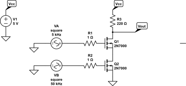
The circuit you have implemented, (if one takes as output, the voltage at the drain of what you label as Q1) is a NAND gate. If both inputs are high, the output is low. Otherwise, the output is high.
Similarly, the steady state output when the gate of Q1 is low and the gate of Q1 is high, is a high output.
But when you change both inputs in opposite directions at the same time, or near the same time, you get a glitch. The output goes low, or attempts to go low, and the current through R3 goes up, or attempts to go up.
In the state just prior to the appearance of (the larger) current glitches shown circle in the images below, the gate of Q1 is high and the gate of Q2 is low. At the moment of the glitch, the gate of Q1 switches to low, and the gate of Q2 switches to high.
 The steady state output when the gate of Q1 is high and the gate of Q1 low, is a high output (very little current through R3).
Changing both inputs to a NAND gate in opposite directions at the same time, or near the same time, creates what is known as a logic hazard. The only safe solution to avoid the glitch is to not switch the inputs in opposite directions at the same time, or near the same time.


simulate this circuitsimulate this circuit – Schematic created using CircuitLab
I implemented the above schematic and set the phase offset of the 5 kHz signal to 2 degrees. This made the glitch much worse.
There are some much smaller current spikes that are caused by some of the gate current being diverted via the gate-drain capacitance into the drain. In the CircuitLab simulation, these are very much smaller current spikes, well under 10 uA, and not really visible in the images I have posted, but visible in blown up images.
FYI, I am not getting the same current values as you in simulation, so I wonder if there is some difference between our circuits, or between our circuits, and the circuit you used to get your results. However, it doesn't really matter for my answer.


