added 194 characters in body
Source Link

I have a device that has a blown up component, and I would like to try and replace it (as well as repairing damaged traces and cleaning up some corrosion) to see if the device still functions.

This is a digital camera released in 1992 (A Dycam Model 3), and I have searched far and wide for a schematic, but have had no luck finding even a hint.

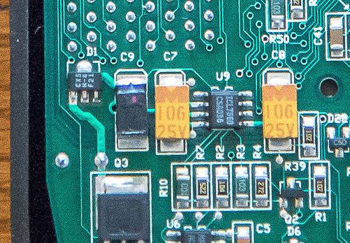
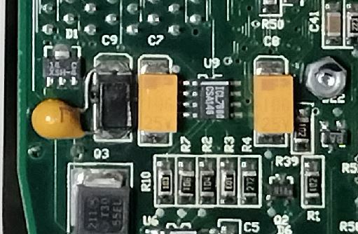
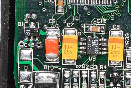
I have found 3 images of similar devices (some from a year or two earlier, some from a year or so later), and they all seem to have the same setup surrounding this failed component.

The ICL7760 chip between the 2 tantalum caps is a voltage converter IC, and the larger SMT Q3 is a MOSFET transistor. I am fairly certain this complex is part of the power supply, or maybe the charging circuit. The device runs on 2x 1.2V NiCd batteries that are recharged in the device itself.

Searching any combination of the numbers and letters visible on the SOT-89 component directly to the left of the blown up device brings up no useful results. I have also searched for the alternative chip seen in one of the images, labeled "SI U", also with no results. I believe based on the "D1" silkscreen, that this SOT-89 chip is a diode of some kind.

The component C9 seems to have an alternate form in the same photo with the alternate SOT-89 chip, as well. The black cubic components on my device and the others in the photos seem to either have small red dots or grooves on their solder pads to indicate polarity. The black cubic package reminds me of a diode, but it is labeled C9 indicating it might be a capacitor. The orange package in the alternative style definitely reminds me of a capacitor. One of the found photos also seems to have a through-hole tantalum capacitor across the pads for the C9 device, which to me makes it look like the C9 device itself is not a capacitor.

I would like to try and identify the D1 chip to help understand what the C9 device is. I am not a whiz with electronics, but have the troubleshooting skills and tools necessary to measure continuity and resistance, but I need some help in understanding what I could measure that would be helpful for identifying these 2 devices.

I am away from my desk right now, but I will measure continuity to determine where the bottom pad of C9 connects to, I suspect one of the left-side pins on the U9 voltage converter IC based on the last image here.

EDIT: I have inspected the datasheet for the ICL7660 IC datasheet, and there are plenty of example circuits shown, but none seem to show what is going on here, at least to my untrained eyes.

Thank you for the guidance!

Close-up view of a portion of a PCB with a square black component that is deformed and visibly burnt

Found photo of a similar undamaged device from an overhead view

Found photo of a similar undamaged device from an overhead view

Found photo of a similar undamaged device with alternate components from an overhead view

I have a device that has a blown up component, and I would like to try and replace it (as well as repairing damaged traces and cleaning up some corrosion) to see if the device still functions.

This is a digital camera released in 1992 (A Dycam Model 3), and I have searched far and wide for a schematic, but have had no luck finding even a hint.

I have found 3 images of similar devices (some from a year or two earlier, some from a year or so later), and they all seem to have the same setup surrounding this failed component.

The ICL7760 chip between the 2 tantalum caps is a voltage converter IC, and the larger SMT Q3 is a MOSFET transistor. I am fairly certain this complex is part of the power supply, or maybe the charging circuit. The device runs on 2x 1.2V NiCd batteries that are recharged in the device itself.

Searching any combination of the numbers and letters visible on the SOT-89 component directly to the left of the blown up device brings up no useful results. I have also searched for the alternative chip seen in one of the images, labeled "SI U", also with no results. I believe based on the "D1" silkscreen, that this SOT-89 chip is a diode of some kind.

The component C9 seems to have an alternate form in the same photo with the alternate SOT-89 chip, as well. The black cubic components on my device and the others in the photos seem to either have small red dots or grooves on their solder pads to indicate polarity. The black cubic package reminds me of a diode, but it is labeled C9 indicating it might be a capacitor. The orange package in the alternative style definitely reminds me of a capacitor. One of the found photos also seems to have a through-hole tantalum capacitor across the pads for the C9 device, which to me makes it look like the C9 device itself is not a capacitor.

I would like to try and identify the D1 chip to help understand what the C9 device is. I am not a whiz with electronics, but have the troubleshooting skills and tools necessary to measure continuity and resistance, but I need some help in understanding what I could measure that would be helpful for identifying these 2 devices.

I am away from my desk right now, but I will measure continuity to determine where the bottom pad of C9 connects to, I suspect one of the left-side pins on the U9 voltage converter IC based on the last image here.

EDIT: I have inspected the datasheet for the ICL7660 IC datasheet, and there are plenty of example circuits shown, but none seem to show what is going on here, at least to my untrained eyes.

Thank you for the guidance!
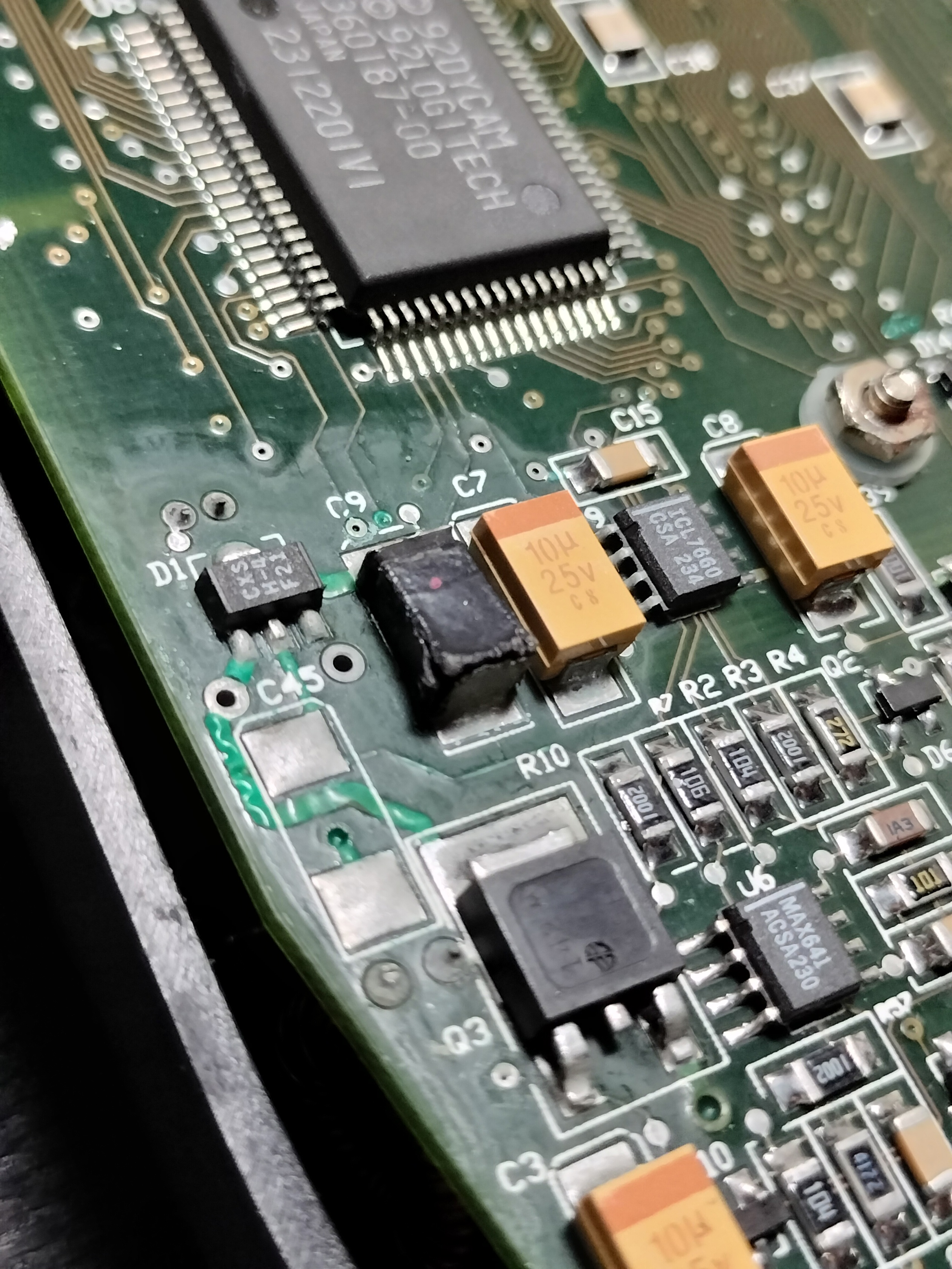
Close-up view of a portion of a PCB with a square black component that is deformed and visibly burnt

Found photo of a similar undamaged device from an overhead view

Found photo of a similar undamaged device from an overhead view

Found photo of a similar undamaged device with alternate components from an overhead view

Source Link

Identifying blown-up SMD component based on surrounding chips and found photos of similar devices

I have a device that has a blown up component, and I would like to try and replace it (as well as repairing damaged traces and cleaning up some corrosion) to see if the device still functions.

This is a digital camera released in 1992 (A Dycam Model 3), and I have searched far and wide for a schematic, but have had no luck finding even a hint.

I have found 3 images of similar devices (some from a year or two earlier, some from a year or so later), and they all seem to have the same setup surrounding this failed component.

The ICL7760 chip between the 2 tantalum caps is a voltage converter IC, and the larger SMT Q3 is a MOSFET transistor. I am fairly certain this complex is part of the power supply, or maybe the charging circuit. The device runs on 2x 1.2V NiCd batteries that are recharged in the device itself.

Searching any combination of the numbers and letters visible on the SOT-89 component directly to the left of the blown up device brings up no useful results. I have also searched for the alternative chip seen in one of the images, labeled "SI U", also with no results. I believe based on the "D1" silkscreen, that this SOT-89 chip is a diode of some kind.

The component C9 seems to have an alternate form in the same photo with the alternate SOT-89 chip, as well. The black cubic components on my device and the others in the photos seem to either have small red dots or grooves on their solder pads to indicate polarity. The black cubic package reminds me of a diode, but it is labeled C9 indicating it might be a capacitor. The orange package in the alternative style definitely reminds me of a capacitor. One of the found photos also seems to have a through-hole tantalum capacitor across the pads for the C9 device, which to me makes it look like the C9 device itself is not a capacitor.

I would like to try and identify the D1 chip to help understand what the C9 device is. I am not a whiz with electronics, but have the troubleshooting skills and tools necessary to measure continuity and resistance, but I need some help in understanding what I could measure that would be helpful for identifying these 2 devices.

I am away from my desk right now, but I will measure continuity to determine where the bottom pad of C9 connects to, I suspect one of the left-side pins on the U9 voltage converter IC based on the last image here.

Thank you for the guidance!

Close-up view of a portion of a PCB with a square black component that is deformed and visibly burnt

Found photo of a similar undamaged device from an overhead view

Found photo of a similar undamaged device from an overhead view

Found photo of a similar undamaged device with alternate components from an overhead view