Became Hot Network Question
Example image added.
Source Link
Russell McMahon
  • 152.1k
  • 18
  • 218
  • 403

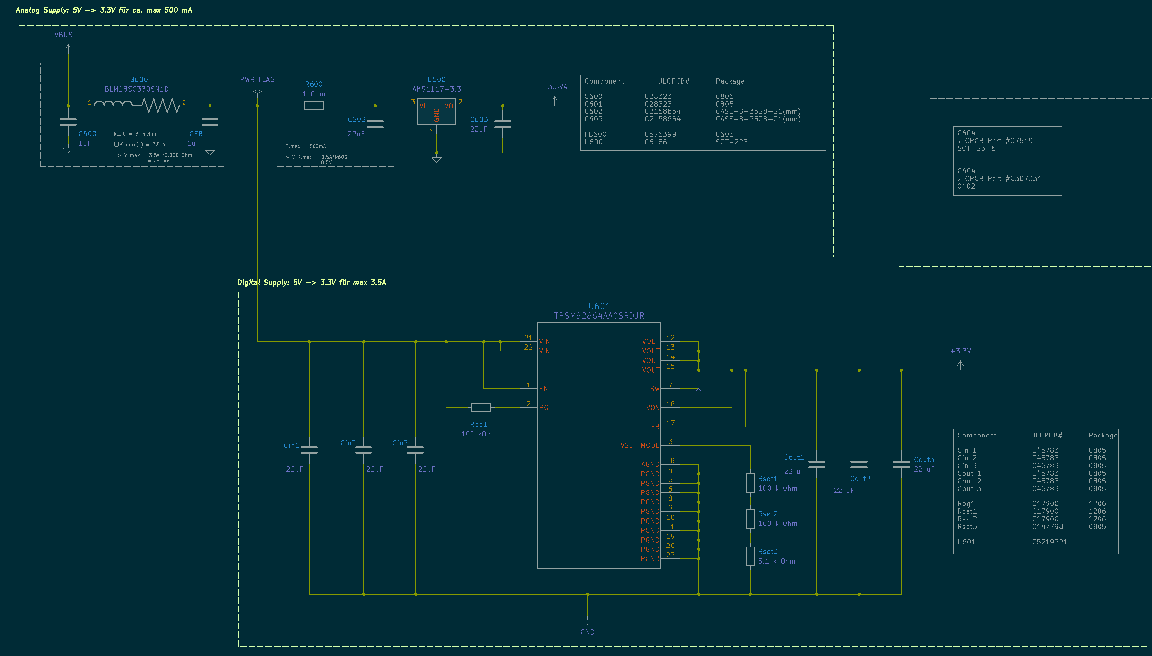
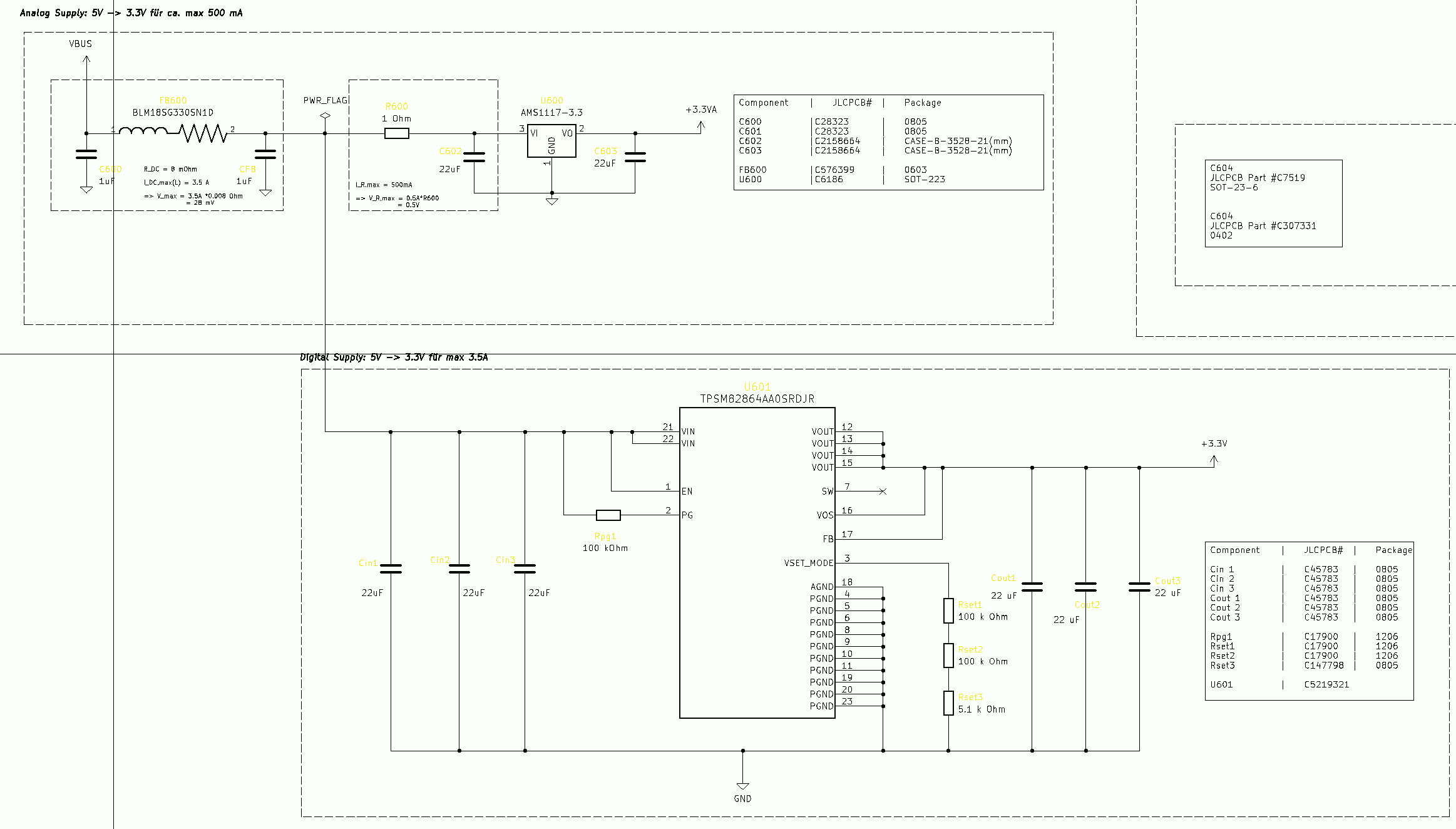
I am creating a mixed signal PCB which has two separate supplies: A buck converter for the digital section and an LDO Regulator for the analog one.

Each regulator steps down 5 V from a USB-C supply to 3.3 V. 
The digital section draws up to 3A, while the analog section draws up to 500 mA.

For the digital side, I am using a TPSM82864AA0SRDJR Buck Converter (lower regulator on the picture, 2.4 MHz switching frequency) and for the analog section, an AMS1117-3.3V, both powered by the VBUS supply line (USB-C, see schematic on the top left).

I have placed a Pi filter consisting of two 1 µF capacitors and a ferrite bead (capable of handling the needed current) in order to suppress the high-frequency noise from the (usually very noisy) USB-C supply rail before reaching my voltage regulators.

I want to ask if this Pi filter arrangement is a good idea considered my regulator setup, or if a different approach would be more appropriate.

Thank you very much in advance.
Greetings,
 Leandro.

enter image description here

enter image description here

Something like this is far more readable. It's not perfect - lines could be thicker and general visibility could be improved, but it gives an idea.

I am creating a mixed signal PCB which has two separate supplies: A buck converter for the digital section and an LDO Regulator for the analog one.

Each regulator steps down 5 V from a USB-C supply to 3.3 V. 
The digital section draws up to 3A, while the analog section draws up to 500 mA.

For the digital side, I am using a TPSM82864AA0SRDJR Buck Converter (lower regulator on the picture, 2.4 MHz switching frequency) and for the analog section, an AMS1117-3.3V, both powered by the VBUS supply line (USB-C, see schematic on the top left).

I have placed a Pi filter consisting of two 1 µF capacitors and a ferrite bead (capable of handling the needed current) in order to suppress the high-frequency noise from the (usually very noisy) USB-C supply rail before reaching my voltage regulators.

I want to ask if this Pi filter arrangement is a good idea considered my regulator setup, or if a different approach would be more appropriate.

Thank you very much in advance.
Greetings,
 Leandro.

enter image description here

enter image description here

Something like this is far more readable. It's not perfect - lines could be thicker and general visibility could be improved, but it gives an idea.
I am creating a mixed signal PCB which has two separate supplies: A buck converter for the digital section and an LDO Regulator for the analog one.

Each regulator steps down 5V5 V from a USBcUSB-C supply to 3.3V3 V. 
The digital section draws up to 3A, while the analog section draws up to 500mA500 mA.

For the digital side, I am using a TPSM82864AA0SRDJR Buck Converter (lower regulator on the picture, 2.4 MHz switching frequency) and for the analog section, an AMS1117-3.3V, both powered by the VBUS supply line (USBcUSB-C, see schematic on the top left).

I  havehave placed a Pi filter consisting of two 1uF1 µF capacitors and a ferrite bead (capable of handling the needed current) in order to supresssuppress the high frequency-frequency noise from the (usually very noisy) USBcUSB-C supply rail before reaching my voltage regulators.

I want to ask if this Pi filter arrangement is a good idea considered my regulator setup, or if a different approach would be more appropriate.

Thank you very much in advance.
Greetings,
  
 Leandro.

enter image description here

I am creating a mixed signal PCB which has two separate supplies: A buck converter for the digital section and an LDO Regulator for the analog one.

Each regulator steps down 5V from a USBc supply to 3.3V. 
The digital section draws up to 3A, while the analog section draws up to 500mA.

For the digital side, I am using a TPSM82864AA0SRDJR Buck Converter (lower regulator on the picture, 2.4 MHz switching frequency) and for the analog section, an AMS1117-3.3V, both powered by the VBUS supply line (USBc, see schematic on the top left).

I  have placed a Pi filter consisting of two 1uF capacitors and a ferrite bead (capable of handling the needed current) in order to supress the high frequency noise from the (usually very noisy) USBc supply rail before reaching my voltage regulators.

I want to ask if this Pi filter arrangement is a good idea considered my regulator setup, or if a different approach would be more appropriate.

Thank you very much in advance.
Greetings,
 Leandroenter image description here

I am creating a mixed signal PCB which has two separate supplies: A buck converter for the digital section and an LDO Regulator for the analog one.

Each regulator steps down 5 V from a USB-C supply to 3.3 V. 
The digital section draws up to 3A, while the analog section draws up to 500 mA.

For the digital side, I am using a TPSM82864AA0SRDJR Buck Converter (lower regulator on the picture, 2.4 MHz switching frequency) and for the analog section, an AMS1117-3.3V, both powered by the VBUS supply line (USB-C, see schematic on the top left).

I have placed a Pi filter consisting of two 1 µF capacitors and a ferrite bead (capable of handling the needed current) in order to suppress the high-frequency noise from the (usually very noisy) USB-C supply rail before reaching my voltage regulators.

I want to ask if this Pi filter arrangement is a good idea considered my regulator setup, or if a different approach would be more appropriate.

Thank you very much in advance.
Greetings, 
 Leandro.

enter image description here

Source Link

USBc rail filtering with ferrite bead for voltage regulators

I am creating a mixed signal PCB which has two separate supplies: A buck converter for the digital section and an LDO Regulator for the analog one.

Each regulator steps down 5V from a USBc supply to 3.3V. 
The digital section draws up to 3A, while the analog section draws up to 500mA.

For the digital side, I am using a TPSM82864AA0SRDJR Buck Converter (lower regulator on the picture, 2.4 MHz switching frequency) and for the analog section, an AMS1117-3.3V, both powered by the VBUS supply line (USBc, see schematic on the top left).

I  have placed a Pi filter consisting of two 1uF capacitors and a ferrite bead (capable of handling the needed current) in order to supress the high frequency noise from the (usually very noisy) USBc supply rail before reaching my voltage regulators.

I want to ask if this Pi filter arrangement is a good idea considered my regulator setup, or if a different approach would be more appropriate.

Thank you very much in advance.
Greetings,
Leandroenter image description here