For the input filter, it's important to have the capacitor close to the supply terminal, with a small loop area to GND. This cap supplies the high-side transient.
This would imply C-L-C-L-C input sequence as shown in the MPQ appnote to be preferred.
Layout matters too: minimize the loop areas for both the main input cap and especially the output cap. TheseThe fast currents in these paths have a profound influence on radiated emissions.
Here's a sim to play with (simulate it here):
You can see that the current ripple at the 5V input is pretty well knocked down by the double-pi filter.
But also take note of transient current going to the FET drain. This has that square/sawtooth shape as the FET switches on and begins to ramp. At first it jumps up immediately, then ramps up with the inductor current build-up. That'sThat initial step is a pretty bitbig dI/dt jump, that's dealt withhandled by the 10uF cap that's closest to the FET. That capcap's performance would be far less effective if thereit were anplaced with the inductor in its path.
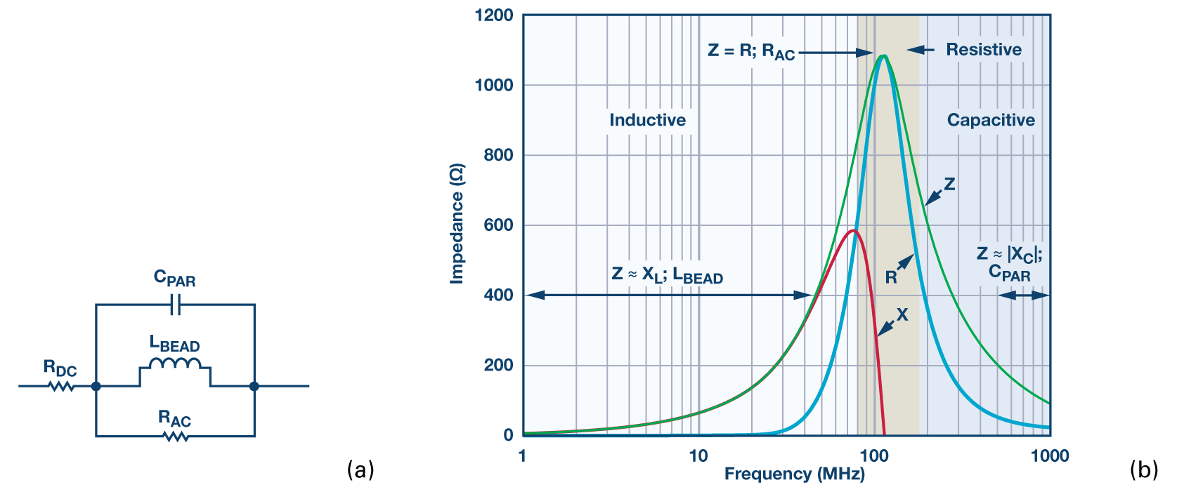
You may be curious how to model a ferrite. The simple model uses 4 components, arranged as below:
From https://www.analog.com/en/resources/analog-dialogue/articles/ferrite-beads-demystified.html
In this article they analyze a selected bead and create a model for it, and show work to optimize its performance with damping.


